|
|


 Arabic
 Bengali
 Chinese
 English
 French
 German
 Hebrew
 Hindi
Hindi Italian
 Japanese
 Korean
 Malay
Malay Polish
 Portuguese
 Spanish
 Turkish
 Ukrainian
 Vietnamese
|
ENCYCLOPEDIA OF RADIO ELECTRONICS AND ELECTRICAL ENGINEERING Microcircuits of the K174 series. Reference data
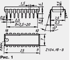
Encyclopedia of radio electronics and electrical engineering / Reference materials DUAL-STANDARD STEREO DECODER KR174XA51 JSC "Angstrem" (Moscow) has developed and mastered in production the chip KR174XA51 - a stereo decoder designed for decoding a stereo signal both according to the domestic standard with polar modulation (OIRT) and according to the foreign one - with a pilot tone (CCIR) in household radios. The microcircuit uses new technical solutions, which are recorded in the Civil Code for Inventions. The microcircuit is framed in a 2104.18-B package (Fig. 1). Weight - no more than 3 g. Implementation technology - planar epitaxial 2 µm BiCMOS with combined oxide insulation and pn-junction.
The KR174XA51 stereo decoder implements XNUMXx oversampling time division decoding to effectively suppress overtones, provides additional pilot tone suppression, constant level shift suppression between channels when decoding a polar-modulated stereo signal to reduce interference when switching "Stereo" - "Mono" and expansion of the dynamic range, as well as the possibility of both automatic recognition of the decoding system and its forced setting, indication of the selected system. If necessary, the stereo decoder can be switched to a permanent "Mono" mode. When using frequency-setting elements with tight tolerances, the microcircuit does not require tuning the frequency of free vibrations of the VCO. The stereo decoder has a VCO frequency control output (62,5/76 kHz), contains a current amplifier for connecting the LED indicator of the "Stereo" mode. (Here and below, through a slash, the frequency values \uXNUMXb\uXNUMXbare indicated for two decoding systems - with polar modulation and pilot tone, respectively). For the operation of a stereo decoder, a minimum of external attachments is required. Pinout of the microcircuit: pin. 1 - feedback signal input; terminal for connecting integrating capacitors of the PLL filter; pin. 2 - feedback signal input; output for connecting a resistor and an integrating capacitor of the PLL filter; pin. 3 - output of the phase detector; output for connecting a resistor and an integrating capacitor of the PLL filter; pin. 4 - general; negative power output; pin. 5 - output for connecting the VCO frequency-setting capacitor; pin. 6 - output for connecting a frequency-setting resistor and a VCO blocking capacitor; VCO control input; pin. 7 - signal output for indication of "Stereo" mode; VCO frequency control signal output; pin. 8 - control signal input of the decoding system selection switch; pin. 9 - output signal AF channel B; pin. 10 - output signal AF channel A; pin. 11 - output of the preamplifier of the AF channel B signal; pin. 12 - inverting input of the low-pass filter amplifier for pre-distortion correction in the polar modulation mode; pin. 13 - non-inverting input of the low-pass filter amplifier for pre-distortion correction in the polar modulation mode; pin. 14 - output of the preamplifier of the AF channel A signal; pin. 15 - positive power output; pin. 16 - input of a complex stereo signal; pin. 17 - blocking output, setting the gain of the scaling amplifier of the complex stereo signal; inverting input of the scaling amplifier; pin. 18 - output of the subcarrier/pilot tone amplitude detector; Schmitt trigger input of the "Stereo" - "Mono" mode selection channel. The functional diagram of the stereo decoder is shown in fig. 2, and a typical circuit for its inclusion is in fig. 3.
The complex stereo signal is fed to the input of the scaling amplifier DA1, which serves to bring the input voltage to the nominal level of the decoder 200...250 mV. Further, the signal passes to the input of the phase detector and the input of the stereo signal decoder. The second input of the phase detector receives an exemplary signal from the shaper of the control pulses. The exemplary signal has either a subcarrier frequency or a pilot tone frequency. The output of a phase detector is proportional to the phase shift between the input and reference signals of the phase detector; it also contains other combinational components in a wide frequency spectrum. To isolate the useful component, a proportionally integrating PLL filter is used, made on an operational amplifier DA2 with external integrating capacitors (C5, C6 in Fig. 3) in the OS circuit. In addition, the filter forms the frequency-phase response of the PLL loop, ensuring its stability and the necessary parameters of the capture bandwidth. The integrated phase error voltage taken from the PLL filter using a DA3 differential amplifier with a current output is applied to the VCO control input. The VCO output pulses with a nominal frequency of 500/608 kHz are fed to the control pulse shaper, which, after recalculation and decoding, generates the decoder control signals and the exemplary signal for the phase detector, thus closing the PLL loop. The stereo signal decoder is made on four fetch/hold blocks - two per channel. The control pulse shaper provides a phase shift of the sample pulses, synchronizing them with the maxima and minima of the subcarrier voltage, to detect the envelopes of channels A and B, respectively. The decoder also contains analog multiplexers-interpolators of channels A and B, which perform signal resampling. In addition, they provide a transition to the "Mono" mode by applying a signal from the decoder input to its outputs, bypassing the decoding blocks. The decoded signal takes the form of 31,25/38 kHz steps. Oversampling consists of adding intermediate points between adjacent signal samples so that the amplitude of the steps is halved and their frequency doubled (up to 62,5/76 kHz). Thus, after filtering by the output RC filters R6C12 and R7C13, a fourfold reduction in the level of overtone noise in the output signal was achieved. From the outputs of the decoder, signals A and B are fed to the inputs of the buffer voltage followers DA4, DA6 (Fig. 2) and then through the adder amplifiers DA7, DA8 to the output of the microcircuit. Filters R6C12 and R7C13 are used to compensate for high-frequency signal pre-distortion with a time constant tf=R6C12=R7C13=50 µs. To obtain tf=75 µs, it is necessary to correct the values of the capacitors, or, if necessary, to introduce electronic switching elements of the time constant. When decoding a polar modulated stereo signal, the low-frequency pre-distortion of the difference channel (A-B) is corrected by a low-pass filter with differential input and output, consisting of an external RC circuit R3C10R4 and an internal amplifier DA5 with a current output. The DA5 amplifier automatically turns on in polar modulation and "Stereo". Time constant tnch =(R3+R4)C10=1,0186 ms. Amplifier gain U1-3/U10-9=4, where U1-3 and U10-9 are the voltage on the corresponding pair of microcircuit pins. The amplitude synchronous detector converts the pilot tone/subcarrier to a DC voltage and integrates them on an external capacitor C2 (Fig. 3), filtering out the audio components. The integrated DC voltage is used to cancel out almost zero pilot tone/subcarrier in the signal chain using negative feedback. The output signal of the amplitude detector also goes to the input of the Schmitt trigger, which, with a sufficient signal level, switches the entire KR174XA51 stereo decoder from the "Mono" mode to the "Stereo" mode. The decoding systems switch is based on an infra-low frequency generator with an RS trigger. In the absence of stereo signal recognition, the stereo decoder periodically switches from working on polar modulation (PM) to working with a pilot tone (PT) and vice versa. After capturing the subcarrier/pilot tone and generating a "Stereo" signal with the Schmitt trigger, the infra-low frequency generator stops and the RS trigger holds the stereo decoder in the recognized decoding standard. Thus, there is an "automatic tuning" to the received signal. The indicator current amplifier provides the possibility of direct connection to the stereo decoder of the LED indicating the operation in the "Stereo" mode. The output of the amplifier - pin 7 - is used to control the frequency of free vibrations of the VCO. During the tuning of the VCO, the LED is turned off. Main characteristics at Tacr.av=25+5°С and modulation frequency 1 kHz
The "Stereo" (A + B) mode is characterized by the presence of both AF components in the complex stereo signal - both in channel A and in channel B. The record "Stereo" (A + B), A, B means that, according to the measurement conditions, they are first fed to stereo decoder, the full stereo signal, and then alternately zero out the component B and then A, respectively. In the "Stereo" (A+B) mode, 0 first a full stereo signal is applied, after which both components are reset to zero; while the subcarrier remains. Such test conditions for stereo decoders are dictated by the features of the PLL loop and are necessary to ensure reliable capture of the stereo signal. It should be noted that electrically the microcircuit is able to withstand without negative consequences the supply voltage up to 8 V, the voltage of the complex stereo signal up to 0,5 V and the output current of the AF through channels A and B up to 5 mA, but the performance of the stereo decoder in this mode is not guaranteed. To minimize noise, especially when receiving weak stations, it is recommended to turn on a low-pass filter with a cutoff frequency of 70 ... 80 kHz at the input of the stereo decoder (at least the simplest passive R1C1 shown in a typical switching circuit). The most effective are active low-pass filters of the 2nd-4th order. Suppression of noise and spurious out-of-band signals prevents their conversion during decoding into the region of the audio spectrum and thereby approaches the maximum achievable noise parameters. Since the frequency band of the CSS is much wider than the bandwidth of the AF (moreover, a limited low-frequency filter with a time constant tf = 50 μs, which corresponds to 3,2 kHz), the accompanying CSS and the noise decoded together with the stereo signal is 10 ... 18 dB higher than with monophonic reception . Therefore, when receiving signals below the level at which the original mono signal-to-noise ratio drops to 48 ... 40 dB, it is necessary to force the stereo decoder to "Mono" mode to maintain acceptable sound quality. To do this, use the signal of the field strength indicator (signal level), which is available in most microcircuits of the radio receiving path. When using an input filter, the channel separation deteriorates the more, the higher the unevenness of the frequency response and group delay in the KSS band from 20 Hz to 53 kHz. So, when working with the simplest R1C1 filter (Fig. 3), the actual channel separation deteriorates to 24 dB for PM and up to 20 dB for FET. In addition, it is necessary to minimize the unevenness of the frequency response not only in the upper (overtone frequency), but also in the lower parts of the frequency spectrum. The values of the input separating (C4 in Fig. 3) and blocking (C3) capacitors, which are excessively large in terms of bandwidth, are necessary to ensure high channel separation. Adjustment of the output signal level to the nominal value of 200...250 mVeff is performed by connecting an additional resistor in series with the capacitor C3. In this case, the transfer coefficient of the scaling amplifier DA1 (Fig. 2) varies within 1...5 in accordance with the formula: Кп=1+20/(5+Rdop), where Rdop is the resistance in kiloohms of the additional resistor. Elements C8, R5 set the frequency of free oscillations of the PLL VCO. With a time constant tf=R5C8=0,94 µs +1% frequency adjustment is usually not required. With the worst accuracy of the ratings of these elements, it is recommended to make the resistor R5 in the form of a series connection of a constant resistor with a resistance of 4,3 kOhm and a variable one - 1 kOhm. When adjusting the frequency of the VCO, the frequency of the signal at pin 7 of the microcircuit is controlled. The LED is turned off for this time, and pin 8 is connected to a common wire. The frequency of the controlled signal should be equal to 62,5 kHz. Capacitor C9 somewhat reduces the effect of interference on frequency stability and phase distortion of the signal and can be eliminated if necessary. When using a power supply with a voltage other than 6 V, it is recommended to adjust the value of the resistor R5 in accordance with the graph of the deviation of the VCO frequency from the supply voltage (Fig. 4).
The value and sign of the resistor correction (in percent) must be equal to the frequency deviation (in percent) at the corresponding point on the graph. DUAL-STANDARD STEREO DECODER KR174XA51 The required value of the time constant tph can be obtained with other ratings of the elements R3, C10, R4. It should only be assumed that the total resistance R3 + R4 should be in the range of 20 ... 50 kOhm. With an error of tHF greater than 2%, the channel separation in the polar modulation mode deteriorates to AF below 1 kHz, which is subjectively imperceptible to the ear to certain limits. The inequality of the resistance values of the resistors R3, R4 has practically no effect on the output parameters, which can be used when selecting ratings from a typical range or setting tf to the maximum separation. Capacitor C11 sets the time interval during which the presence of a signal of one or another coding standard is checked one by one. The decoding standard is forced by connecting pin 8 of the chip with a common wire for polar modulation and with a positive power wire for pilot tone. In Auto Decode System Detect mode, the high and low voltage levels on this pin can be used to indicate the selected decode system for the received signal. To do this, it is necessary to provide a high input resistance of the indicator - more than 1 MΩ. Capacitor C2 sets the integration time constant of the amplitude detector. Its decrease can lead to a deterioration in the separation of channels into AF in a system with polar modulation and erroneous definitions of a stereo signal, and an increase can lead to an increase in the identification time. The identification time, in turn, must be less than the time interval allotted for identification. The stereo decoder can be forced into mono mode by connecting pin 18 to ground through a 68 kΩ resistor. In practice, it is more convenient to implement this function using a node, the diagram of which is shown in Fig. 5. If the output voltage of the AF is set at a level of more than 250 mVeff, then the value of the resistor R2 should be reduced.
LED HL1 must have a minimum forward voltage drop. Only red LEDs with acceptable brightness at a current of 0,5 mA are suitable here. Otherwise, the LED will have to be turned on through a current buffer amplifier according to the circuit in Fig. 6. The same buffer stage can be used to generate a logical TTL/CMOS "Stereo" signal. It is removed from the collector of transistor VT1 (resistor R2 should be replaced with another one, with a resistance of 100 kOhm). The presence of the "Stereo" signal corresponds to a low logic level at the output of the buffer stage (on the collector of transistor VT1).
When mounting a microcircuit on a board, one should take into account the high sensitivity of the phase detector to leakage currents and avoid flooding pins 1 and 2 of the microcircuit with flux. Good results in this regard are obtained by using a protective ring made by a printed conductor connected to pin 3. The ring should surround pins 1 and 2, as well as the pins of elements R2, C5, C6 (Fig. 3). In addition, to minimize the interference emitted by the microcircuit, the filter capacitor C7 of the power supply should be located as close as possible to its terminals 4 and 15, and the elements R5, C8, C9 - to terminals 4, 5 and 6. On fig. 7 shows the dependence of the minimum output signal level, at which the stereo decoder switches to the "Stereo" mode, on the supply voltage for both decoding standards. The output current-voltage characteristic of the "Stereo" mode indicator (according to pin 7 of the stereo decoder) is shown in fig. 8. Here, in the section Uind \u1,4d 2 ... 62,5 V, the output leakage current with a frequency of 76 / 2,2 kHz has a pulse shape close to a meander. With a further increase in the indicator voltage, the amplitude of the current pulses decreases and at Uind = XNUMX V or more, the indicator current becomes constant and leaky.
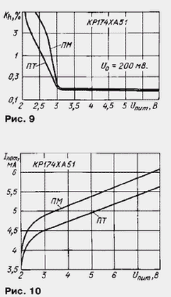
The dependences of the coefficient of non-linear distortion and the current consumed by the stereo decoder on the supply voltage are shown in fig. 9 and 10 respectively.
Author: S.Alenin, Moscow
Traffic noise delays the growth of chicks
06.05.2024 Wireless speaker Samsung Music Frame HW-LS60D
06.05.2024 A New Way to Control and Manipulate Optical Signals
05.05.2024
▪ Compact computer MINISFORUM GK50 ▪ Multitasking reduces brain productivity
▪ section of the site Calls and audio simulators. Article selection ▪ article What are sardines? Detailed answer ▪ Animal care worker at the zoo. Standard instruction on labor protection ▪ article The blacker, the lighter. physical experiment
Home page | Library | Articles | Website map | Site Reviews
www.diagram.com.ua |


 Leave your comment on this article: