|
|


 Arabic
 Bengali
 Chinese
 English
 French
 German
 Hebrew
 Hindi
Hindi Italian
 Japanese
 Korean
 Malay
Malay Polish
 Portuguese
 Spanish
 Turkish
 Ukrainian
 Vietnamese
|
ENCYCLOPEDIA OF RADIO ELECTRONICS AND ELECTRICAL ENGINEERING Switching power supply for UMZCH. Encyclopedia of radio electronics and electrical engineering
Encyclopedia of radio electronics and electrical engineering / Transistor power amplifiers The advantages of a switching power supply in comparison with a classic-type network power supply unit with a power of 150 W are obvious: significantly less weight and dimensions. With the correct design and installation, any noticeable interference and the background of the AC mains are excluded both in the UMZCH and in the audio system as a whole. A detailed description of the establishment of a pulsed power supply will also be useful in the manufacture of a more powerful converter with several output voltages. To be or not to be switching power supplies (SMPS) in UMZCH? Such a sacramental question in relation to this class of devices is by no means accidental. This is also evidenced by the discussion of radio amateurs on the forum of the journal's website, dedicated to the publication [1]. Most of the participants in the discussion still consider it justified to use SMPS in UMZCH. But there is a drawback in the design of the SMPS pulse transformer [1], which the participants in the discussion did not pay attention to at all. Its primary winding is wound in two wires. Although the magnetic coupling of the turns in this case is maximum, it is achieved in a risky way. In all adjacent turns, the effective potential difference reaches the rectified mains voltage (about 300 V). Lacquer insulation of conductors is able to withstand such an impact, but what can happen to it after a few years of operation? Even in the absence of an overlap of conductors (and this is not excluded), their inevitable mechanical displacement during heating and cooling after each switch-on can significantly weaken the dielectric strength of the insulation, and then ... at best, the fuse will “burn out”. In this case, the use of the PELSHO wire instead of the PEV-2 recommended by the author is more justified. In general, the proposed circuit design is quite viable. Some advantage (with the exception of the limiting conversion power) over the pulse converter proposed in [1] is provided by flyback SMPS. Only one switching transistor, effective stabilization of the output voltage with changes in the mains voltage and load, high manufacturability of the windings for the W-shaped magnetic circuit compared to the ring (toroidal) - these are far from the full range of advantages of such a converter. About four years have passed since the publication of the mentioned article, during this period other circuitry variants of the SMPS have been proposed in the journal, in particular [2-4]. In the same article, I propose a variant of such a device with a multi-channel output. The main parameters
The rms value of the output voltage ripple was measured with a VZ-48A millivoltmeter. The operating range of the input voltage characterizes the possibility of both long-term operation of the SMPS in the specified interval, and the ability to neutralize short-term dips and surges in the mains voltage without degrading the given parameters. However, it should be remembered that the device cannot be turned on at a mains voltage below 170 V. The flyback converter operates in an intermittent magnetic flux in a pulse transformer, the maximum duty cycle of switching pulses is 0,45 (at the minimum mains voltage). More powerful output voltage rectifiers (channels 1, 2) are designed to power the output stages of the bridge UMZCH, and low-power (channels 3, 4) - for the input amplifier circuits on the op-amp. Device and construction Consider the operation of the device according to the circuit diagram shown in Fig. one.
Both the circuit itself and the elements used with their possible replacement were described in detail in [2–4], and no additional comments are required here. However, it is necessary to describe in more detail the method used here for switching on the secondary control loop, since it is important to take into account its features when setting up an SMPS. With slight simplifications, the process of stabilizing the output voltage through the secondary feedback loop can be represented as follows. As a tracking element in similar devices, a so-called parallel-type stabilizer is used - a DA2 KR142EN19A microcircuit (import analogue - TL431 with any letter index). The load of the microcircuit is the parallel-connected ballast resistor R17 and the emitting diode (terminals 1, 2 of the optocoupler U1) with the current-limiting resistor R18. The ballast resistor creates the minimum load necessary for the normal functioning of the microcircuit. The output voltage through an adjustable resistive divider R14-R16 is applied to the control input of the microcircuit (pin 1). To ensure a margin of regulation, the divider is calculated so that at the control input of the microcircuit at the nominal output voltage of the SMPS, the voltage interval set by the tuning resistor R15 is about 2,5 ± 0,25 V. Suppose that at the peak of the volume of the phonogram, the current consumed by the UMZCH will sharply increase, and due to the increased voltage drop across the IVa winding and the VD6 rectifier diode, the output voltage of the +35 V source will decrease. Accordingly, the voltage at the control input of the DA2 microcircuit (pin 1) will decrease, and the current through the ballast resistor and the emitting diode will sharply decrease. The equivalent resistance of the collector-emitter section of the phototransistor optically coupled to the emitting diode will increase. Since this resistance is connected in parallel with the resistor R3, which is the upper arm of the resistive voltage divider, the voltage at the input of the error signal amplifier (+2,5 V at pin 2 of DA1) will decrease. The error signal amplifier will immediately compensate for such a decrease in the input voltage by increasing the duty cycle of the switching pulses and thereby restore the previous voltage value at the output of the device. The features of the device should also include the multi-channel output voltage sources. Control and regulation of the output voltage is carried out only in one channel, but a strong magnetic connection between all secondary windings allows you to effectively stabilize the voltage in each channel with one PWM controller. The printed circuit board of the device is shown in fig. 2.
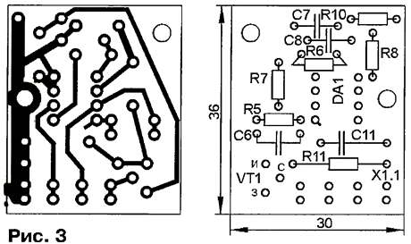
Among the design features of the IIP, the following should be noted. The SHI controller node A1 (the drawing of its board is in Fig. 3) is connected to the main board using a four-pin unified connector X1, similar to those used in USCT TVs. The fixing screws between the main board and the heat sink provide its electrical connection with the common wire of the SMPS. The switching transistor VT1 is installed through a mica plate on a ribbed heatsink with dimensions of 70x45x24 mm. The controller board A7,5 is attached to the same heat sink with two screws on tubular racks 1 mm high. The DA1 microcircuit, installed in the board through the adapter panel, is firmly pressed against the heat sink by the heat sink surface of the case. The use of KPT8 heat-conducting organosilicon paste allows the controller to monitor the operating temperature of the transistor and automatically turn off the SMPS in emergency situations when it overheats. When mounted on the A1 board, the VT1 transistor is soldered with preformed leads so that its plane is parallel to the board surface, and the metal flange of the transistor case faces the heat sink connected by a clamping plate and two additional screws. The A1 board itself also faces the heat sink with the side where the elements are located. Capacitors C9, C10 are soldered directly to the corresponding contacts of the panel from the side of the printed conductors.
On the main board, the optocoupler U1 is also installed through the adapter panel. A voltage of +35 V is supplied to the secondary control circuit through a heat sink electrically connected to the cathode of the VD6 diode, which made it possible to do without an additional jumper on the printed circuit board. In the author's version, a ribbed radiator with dimensions of 40x20x18 mm was used, such were previously made for P213-P217 transistors. As a heat sink, you can also use U-shaped aluminum rolled products with a thickness of 1,5 ... 2 mm and dimensions of 100x40 mm. The diode is soldered into the board so that its metal flange, electrically connected to the cathode, faces the heat sink, and then pressed with two screws. The same heat sink is suitable for the VD7 diode. The device does not need additional forced cooling. Trimmer resistor R15 - type SPZ-16V. With the selected oxide filter capacitors (CarXon series or similar), the required level of output voltage ripple is fully provided by standard high-frequency chokes, and there is no need to make home-made ones. Chokes DM-2 are used in 35x2,4 V channels, and DM-2 in 15x0,6 V channels. All these chokes are installed perpendicular to the main board. For the inductor L2, a 10 mm piece of tubular ferrite is used, which is used, in particular, in the named inductors. A PEV-2 0,72 wire is threaded through the axial hole in the tube, and then each end is bent 180 ° from its original position, thereby forming a closed loop. This inductor effectively suppresses high-frequency oscillations that occur in the transformer when the switching transistor is turned on and off, and also eliminates self-excitation in control loops. The pulse transformer of the device and its other main elements are calculated using the specialized program VIPer Design Software, described in detail in [4]. The inductance of the primary winding of the transformer at a conversion frequency of 50 kHz should correspond to 420 ... 450 μH. The printed circuit board of the device was initially designed for a transformer with a magnetic circuit Sh10x10 made of M2500NMS1 ferrite with a standard contact panel (pin numbers 1'-6', 7-12). But then the board was supplemented with pads 1-6. The problem of selecting a transformer as one of the main elements that determine the reliability of the entire device arose for the author due to the fact that in one of the metropolitan firms, under the guise of a Sh10x10 magnetic circuit made of M2500NMS1 ferrite, he was sold a magnetic circuit of the same size without factory marking. In the transformer, it warmed up so much that the temperature rise clearly did not fit into the design tolerance. The operating frequency of the conversion was varied and, accordingly, the number of turns, the order of the windings, the diameter of the conductors, and all to no avail. As the volume of negative results accumulated, the idea matured to compare the electrical resistance of the existing magnetic circuit with ferrite M3000NMS2 (W 12x20). The measurement results confirmed the guess: the electrical resistance measured by the Ts4341 device did not depend much on the relative position of the applied measuring electrodes, and for the material of the "fake" magnetic conductor it amounted to 0,9 ... 1,2 kOhm, and for the M3000NMS2 ferrite - 2 ... 3 kOhm The reference literature indicates that the electrical resistivity of M2000NM1 is 0,5 Ohm-m, and M2500NMS1 (M3000NMS2) is 1 Ohm-m. As a result, one of the companies selling imported components, among the many components, chose the cheapest pulse transformer for SAMSUNG TVs (decimal number P/N 5106-061101-00) with a magnetic circuit size ER42/22/15 and a non-magnetic gap of 1,3 mm (measured inductance factor of about 180 nH per turn). The specific electrical resistance of the material turned out to be almost the same as that of ferrite M3000NMS2 (W 12x20). For use in the IIP of such and other ready-made transformers, the following technological operations are performed. Before disassembly, the electrostatic screen is removed from the transformer, and then completely immersed in acetone or another solvent and kept in it for three days. After such an operation, the frame with windings should move along the central core of the magnetic circuit without applying significant efforts. This magnetic core is clamped in a vise through cardboard spacers from the side opposite to the terminals. Two powerful soldering irons heat up to 100 ... 120 ° C the places of gluing the joints of the two halves of the magnetic circuit, and through the U-shaped mandrel apply a slight blow with a hammer on the frame with the windings towards the transformer leads. As a result of the impact, the halves of the magnetic circuit should separate. It remains to rewind the windings in accordance with the data given in the article. A significant margin in the cross section of the magnetic circuit window allows the use of winding wires of a larger diameter and, if necessary, to increase the output power of the SMPS. It is also possible to use a transformer with a magnetic circuit Ш12x20x21 made of M3000NMS2 ferrite, used in switching power supplies for USCT TVs. Moreover, the output power of the SMPS in this case can be significantly increased without altering the electrical part of the device. But a transformer with a rated power of 120 W (maximum 180 ... 200 W) will have to be calculated according to the recommendations of Yu. Semenov [2]. In this modification, some elements on the board will have to be slightly shifted. On the magnetic circuit from the pulse transformer of the PSU of the SAMSUNG TV, used by the author, 17 turns are first laid in two PEV-2 0,57 wires (winding la), then, after interwinding insulation, windings IV6 and IVa are wound (second and third layers - 21 turns each) wire PEV-2 1,0, and again winding insulation. In the fourth layer, in two wires PEV-2 0,41 "discharged" - 9 turns of the windings Shb and Sha. After interwinding insulation, the 5th layer is 8 turns with wire PEV-2 0,12 (again "in a discharge") of winding II. The 6th and 7th layers are winding 16, consisting of 17 and 16 turns, respectively, into two PEV-2 0,57 wires. Sections la and 16 of the primary winding are connected by soldering the corresponding pins on pin 2 (2'), which is shortened by a few millimeters so that it does not interfere with the installation of the transformer on the board. Conclusion 2 is not soldered to the board. After gluing the magnetic core, a screen is installed on the finished transformer - a coil of copper foil 15 mm wide, covering the middle part of the coil. As experiments with other magnetic circuits have shown, when using the Sh10x10 (M2500NMS1) magnetic circuit with a non-magnetic gap of about 1 mm, the number of turns in the windings will be the same as for the "Korean" magnetic circuit. Moreover, a constructive non-magnetic gap of 1 mm on the central core can be replaced with 0,5 mm thick getinax spacers between the side rods of a conventional magnetic circuit. At the same time, the leakage inductance of the transformer increases from 4 to 6 μH, but the voltage surge at the drain caused by it at the moment the switching transistor IRFBC40 is turned off is still far from its limit value of 600 V. Establishing a UPS If the installation of the device is carried out without errors and serviceable elements are used, its adjustment comes down to setting the output voltage (selecting the operating mode of the optocoupler). However, it is impossible to completely exclude the possibility of the failure of the SMPS when it is first turned on, so we will consider the adjustment process in more detail. The information given here will also be useful when setting up a self-designed SMPS with other output voltages. First of all, before installing a field effect transistor, make sure that it is working. How to do this was described in detail, for example, in [5] and other articles published in the journal. Then, with the help of a universal device for testing the SMPS [5], with the controller node A1 turned off, the correct phasing of the transformer windings and the operability of the output rectifiers are checked. In order for the operating frequency of the device to correspond to the required conversion frequency (50 kHz), it is enough to solder another 220 pF capacitor in parallel to the 120 pF frequency-setting capacitor in the device. In this case, the output voltages of the SMPS will approximately correspond to the required ones. At the output of the device, resistors are included, the resistances of which are approximately equivalent to half the load. In each of the 2x15 V channels, these can be incandescent lamps with an operating current of 0,1 ... 0,2 A, allowing you to visually control the appearance of output voltages. In 2x35 V channels, two resistors connected in series with a resistance of 33 Ohm (PEV 25 W) are used as a load. The next step is to check the health of the controller and control the functioning of the SMPS with the primary control loop, for which the secondary circuit is temporarily turned off by setting the slider of the resistor R15 to the lower position according to the diagram and removing the optocoupler U1 from the panel. When establishing a SMPS, it is necessary to constantly monitor the output voltage with a voltmeter. Its value of 36 V is the maximum allowable for the DA2 chip, and the reverse voltage on the rectifier diodes VD6, VD7 is also approaching the maximum allowable. To identify the electrical strength margin of the device, the author deliberately increased this voltage to 45 V for several minutes. But long-term operation of the SMPS in this mode is impossible due to a sharp decrease in reliability. To check the health of the DA1 microcircuit and monitor the operability of the primary control loop, a "technological" tuning resistor with a nominal value of 3-22 kOhm is soldered to the switching points of the resistor R33 (it is temporarily excluded) with a rheostat, the engine of which is set to the position of maximum resistance, and to the capacitor C13 at this time solder a low-power 18 V zener diode, which will limit the controller supply voltage. With node A1 removed from connector X1, a stabilized voltage of +13 V is supplied to the positive terminal of capacitor C17,5 from a laboratory power supply (LIP), which is necessary for guaranteed switching on of the DA1 chip. Without connecting the SMPS to the network, by rotating the process resistor engine on pin 3 of connector X1, the voltage is set to +2,5 V. After that, node A1 is inserted into the connector and using an oscilloscope, the presence of pulses at the gate of the switching transistor VT1 is monitored. If necessary, by selecting the R6C8 circuit, the frequency of the switching pulses is adjusted. If there are no pulses, replace the DA1 chip. At the next stage, the voltage of the LIP is reduced to +15 V, the voltage of +2,5 V is restored with a process resistor on pin 3 of connector X1, then the LIP is turned off and the SMPS is connected to the network. The increase in the supply voltage of the microcircuit occurs relatively slowly as the capacitor C13 is charged, and a time interval of 0,5 ... 2 s is clearly visible between the supply of the mains voltage and the moment it is turned on. It is possible that for some samples of microcircuits KR1033EU10 (UC3842, KA3842) the supply voltage of the microcircuit will not reach the threshold value of 14,5 ... decrease in the resistance of the resistor R17,5. Smooth movement of the technological resistor engine makes sure that the output voltage of the SMPS can be regulated. At this point, the health check of the DA1 microcircuit and the control of the operability of the primary control loop are completed and proceed to the establishment of the secondary control loop. Any LED is installed in the panel for optocoupler U1 with the anode to pin 1, the cathode to pin 2. In the R18 circuit - pin 1 of the optocoupler, a 15 ... 30 mA milliammeter is turned on (this can be a combined measuring device). A LIP with an output voltage of 35 V is connected to the +35 V output of the SMPS in the appropriate polarity (the load can be turned off in this case). Resistor R18, which determines the value of the maximum output power (twice the nominal value - about 150 W), is pre-selected so that at the highest position of the resistor R15 engine in the circuit, the controlled current does not exceed 12 mA. If the current is significantly higher (in this case, the LED may fail, but it is still cheaper than the optocoupler) and the trimming resistor R15 is not adjustable, replace the DA2 chip. Then, instead of the LED, an optocoupler is installed and the possibility of regulating the input current and its maximum value are again checked. If there is no current, replace the optocoupler. After that, the engine of the resistor R15 is set to the lower position according to the diagram, and the negative output of the LIP is connected to output 2 of the optocoupler. By smoothly increasing the LIP output voltage from zero, the controlled current is set in the range of 1 ... 2 mA. The second LIP is connected to the capacitor C13 and the voltage at its output is set to 12,5 V, while the mains supply of the SMPS must be turned off. By adjusting the process resistor, the voltage on pin 3 of connector X1 is 2,5 V. By changing the current of the emitting diode of the optocoupler within 0,5 ... 3 mA, one is convinced of its strong influence on the previously set voltage of 2,5 V. If this does not happen, replace the optocoupler. The input current of the emitting diode is again set in the range of 0,5 ... 2 mA, and 2,5 V is restored with a technological resistor on pin 3 of connector X1, after which the second LIP with a voltage of +12,5 V is turned off, and the first LIP with an output voltage +35 V is again connected to the output of the SMPS. By smoothly moving the slider of the resistor R15 (upward according to the scheme), the adjustment is stopped at the moment when the milliammeter needle starts to move. The LIP is disconnected from the block and a load equivalent is turned on instead. The SMPS can now be powered up again. When the network is on, the +35 V voltage at the output of the device may differ by tenths of a volt from the required value. Using the method of successive approximation, using the adjustments of the resistor R15 and the technological resistor (they are highly interdependent), the input current of the emitting diode is set to about 1,5 mA, and the voltage at the output of the SMPS is +35 V. Closing the outputs of one of the load resistors (33 Ohms) in the circuit + 35 V, control the decrease in the current of the emitting diode by about 0,5 mA, and when one more of the load resistors in the -35 V circuit is closed, an additional decrease by 0,5 mA. In this case, using an oscilloscope, one can observe a noticeable two-step increase in the duty cycle of switching pulses. In conclusion, LATRom changes the mains voltage in the range of 125 ... 250 V. With all changes in the resistive load and mains voltage, the output voltage of the SMPS should stabilize with an accuracy of no worse than 0,1 V. Then, a milliammeter, a protective zener diode are removed from the device and the technological resistor (R3) is soldered. Measure its effective resistance and solder a resistor with the nearest rating instead. Make sure the required stability of the output voltage. After that, the maximum power provided by the power supply at the rated mains voltage is measured, for which load resistors with a resistance of 33 ohms are connected to the PSU output in parallel - two for each channel. The current in the load is controlled by an ammeter by 3 A. By reducing the resistance of the resistor R18 (in the author's version - up to 680 Ohms), the protection device is turned on at a current of more than 2,5 A when an additional load is connected. Then - at nominal load - it is necessary to restore the changed output voltage of +15 V with a tuned resistor R35. As a result, at maximum load, the output voltage decreases by 2 ... 3 V, depending on the parameters of the microcircuit. This completes the establishment of the secondary control loop. In conclusion, the establishment, observing the precautions, control the pulses at the drain of the field effect transistor VT1. In the presence of high-frequency self-excitation, which can occur, for example, if the terminals of the inductor L2 are closed, in the controlled circuit, in addition to the main inverter pulses, narrow (about 1 μs long) noise pulses will be present. Their spectrum is so wide that they make it difficult to receive radio stations even in the VHF band with a receiver located a few meters from a working SMPS. This method allows you to detect the presence of self-excitation in the device "by ear", without an oscilloscope. After the excitation is eliminated, if necessary, the load is increased to the nominal value and after about half an hour, the steady-state thermal conditions of the transformer, rectifier bridge, switching transistor and diodes in the output circuits are checked. If all parts are in good condition, the temperature of their housings should not exceed the ambient temperature by more than 20 ° C. The imported rectifier bridge purchased for the first author's version of the SMPS turned out to be substandard and overheated strongly even at idle (in the absence of any load connected to the mains rectifier). The reason for such a deficiency can only be detected by measuring the reverse current of the bridge diodes at a voltage of about 300 V. Overheating of the rectifier bridge and its destruction could lead to damage to the remaining elements of the network rectifier, and after them the switching transistor with the controller. The proposed topological version of the device's printed circuit board, with some simplifications, can also be used when replacing the A1 controller assembly with its complete analogue - the imported VIPer100 (VIPer100A) microcircuit. About testing SMPS The parameters of the SMPS given at the beginning of the article were measured in nominal mode with a constant load at the outputs of the power source. Its maximum power can be estimated from the maximum current in the load at the +35 V and -35 V outputs, which reaches 2,5 A when the voltage at these outputs decreases by approximately 3 V. Meanwhile, if an UMZCH with a high output power is connected to the power supply as a load, this will correspond to the dynamic mode. At the peaks of the volume of the amplified audio signal, especially in the frequency band of 20 ... exceeding the nominal value of the current by several times, and in pauses - to weaken to a minimum, limited by the quiescent current of the UMZCH output transistors. It is obvious that the automatic control systems in the microcircuit allow, to some extent, to compensate for the fluctuations in the output voltage associated with the dynamic load. But it is clear that these possibilities are not unlimited, and therefore some buffer is required between the SMPS and the UMZCH, which weakens sudden changes in the load. As such a buffer, additional filter capacitors are used in the power supply channel of each UMZCH arm. If we compare high-frequency switching and conventional mains power supplies, we can assume that the former should have some advantage over the latter, associated with the possibility of using filter capacitors of a smaller capacity. Typically, radio amateurs in traditional PSUs use filter capacitors at the rate of 4700 microfarads for every 50 W of UMZCH power, but sometimes they increase their capacity to many tens of thousands of microfarads. In the opinion of the author, there are no grounds for such an increase in the IIP. After all, the energy supply of filter capacitors in traditional PSUs occurs at a frequency of 100 Hz, and in a SMPS - 50 kHz! Of course, it is not necessary to hope that in this case the capacity can be chosen 500 times less, but it is necessary to find out some of their optimal value. This issue was brought to the fore in the performance tests of this SMPS with a stereo amplifier. The tests were carried out with UMZCH on the TDA7294 chip [6] according to the switching scheme recommended by the manufacturer. The output power of the UMZCH for a rated load of 8 ohms is 60 ... 70 watts. Each channel of the stereo UMZCH with additional filter capacitors of 2200 μF was connected to a bipolar source of ±35 V through high-frequency chokes DM-2,4 (5 μH). Exactly the same chokes were used to connect a bipolar ±15 V source to the tone block. Turning on the UMZCH is virtually silent. The measurements showed that even at the maximum level of the tone signal in the band of 20 Hz ... 50 kHz without noticeable distortion at a load of 8 Ohm, the average current consumed from the source ± 35 V does not exceed 1,1 ... 1,2 A for each of amplifier channels. It should be remembered that the push-pull UMZCH for each of the power supply channels (+35 V and -35 V) consumes a pulsed current with a duty cycle close to two. During the pause, the capacitors of the smoothing filters have time to restore the charge, providing a pulsed load current in the next signal period. At the maximum output power of the UMZCH, the "drawdown" of the voltage relative to the nominal value does not exceed 2 V. Since this mode of testing amplifiers on a tone signal is very far from real operating conditions, in the case of amplification of musical signals, the output voltages of the SMPS remain stable. Literature
Author: S. Kosenko, Voronezh
Machine for thinning flowers in gardens
02.05.2024 Advanced Infrared Microscope
02.05.2024 Air trap for insects
01.05.2024
▪ Smart clothes that track posture and movement ▪ HGST Ultrastar He 6TB Helium Hard Drives ▪ CY25200ZZC - programmable clock generator chip ▪ Smart windows based on the octopus organism
▪ section of the site Civil radio communications. Article selection ▪ article Trumpet of Jericho. Popular expression ▪ article What is sashimi? Detailed answer ▪ article Testing the abrasive tool. Standard instruction on labor protection ▪ article A powerful power supply option. Encyclopedia of radio electronics and electrical engineering
Home page | Library | Articles | Website map | Site Reviews
www.diagram.com.ua |


 Leave your comment on this article: