|
|


 Arabic
 Bengali
 Chinese
 English
 French
 German
 Hebrew
 Hindi
Hindi Italian
 Japanese
 Korean
 Malay
Malay Polish
 Portuguese
 Spanish
 Turkish
 Ukrainian
 Vietnamese
|
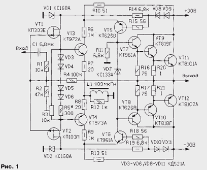
ENCYCLOPEDIA OF RADIO ELECTRONICS AND ELECTRICAL ENGINEERING UMZCH with inductive correction. Encyclopedia of radio electronics and electrical engineering
Encyclopedia of radio electronics and electrical engineering / Transistor power amplifiers The peculiarity of this UMZCH is the inductive correction of the amplifier input stage, as well as a symmetrical structure. Power amplifier, the circuit of which is shown in Fig. 1, contains practically one voltage amplification stage (transistors VT5, VT6) and a three-stage current amplifier (VT7-VT12) with symmetrical. structure, providing a power of at least 4 W at a rated load of 70 ohms. This circuit design made it possible to obtain very good transient characteristics and a wide VD11 bandwidth. transmission. According to the author and other participants in comparative listening, the amplifier reproduces percussion instruments and complex sounds (for example, choral music) very cleanly and naturally.
The voltage amplification stage is a conventional cascode amplifier (OE-OB structure), only in a symmetrical design. It is complemented by an input follower based on field-effect transistors, which reduces the requirements for the bias circuits of the input stage. Its temperature stabilization is ensured by the joint operation of diodes VD3-VD6 and VD8-VD11. Phase-frequency correction in the amplifier is carried out by local feedback loop - inductor L1, connected to the emitters of the input transistors, and resistor R12. Inductance in the input stage plays a significant role in eliminating intermodulation distortion in the presence of supra-tonal and high-frequency components in the signal [1]. Attempts to adjust the amplifier in any other way result in deterioration of the sound - transparency and volume are noticeably reduced. True, this correction method has the disadvantage that the coil is sensitive to magnetic interference. Therefore, it is advisable to wind it on a ring magnetic circuit or shield it (preferably both). Two elements must be installed in this cascade - resistors R15 and R18. Without them, the amplifier is excited, and the final stage transistors may fail. Moreover, without OOS this happens even faster than with it. To simplify the bias circuits and temperature stabilization of the output transistors, the current amplifier is designed with current unloading of the output stage: transistors VT11, VT12 operate with a cutoff (in class C), but the previous pair of transistors operate directly on the load through the very low resistance of resistors R20, R21 (1 Ohm ) and thereby completely eliminates switching distortion. This cascade construction allows you to use a regular zener diode in the bias circuit (VD7) (its TKN is about -0,11%/°C) and not worry about stabilizing the current of the output transistors. In addition, the frequency characteristics are high, since the base-emitter pn junctions of the output transistors are shunted by resistors and the junction capacitances are recharged at the highest possible speed. Structurally, the amplifier is made on a printed circuit board, except for the output transistors (VT7-VT12), placed on radiators without additional insulation. The radiators themselves must be insulated. As inductor L1 (400 μH), the author used two series-connected high-frequency chokes DPM-0,1 with an inductance of 200 μH each. In addition to the elements indicated in the diagram, the following parts can be used in the UMZCH: VT3, VT4 - transistors KT972B, KT973B; VT9, VT10 - KT819V, KT818V; VT11, VT12 - KT8101B, KT8102B; VD1, VD2 - KS175A; VD3-VD6, VD8-VD11 - KD522 series or other similar ones. The selection of a pair of complementary field-effect transistors VT1, VT2 is carried out separately as follows. The source circuit of each of them (between the source and gate terminals) includes two low-power silicon diodes (in the forward direction), which act as a bias voltage source; a milliammeter is included in the drain circuit. When a supply voltage within 4...9 V is applied to them (with polarity corresponding to the structure of the transistor), the drain current is measured. A pair of transistors with a quiescent current of 1...2 mA and a current difference of no more than 15% is suitable, although the zero-setting elements at the output (R2, R3) allow the use of pairs of transistors with a larger current difference. The UMZCH is adjusted by selecting resistor R5 until approximately the same current is obtained (5...6 mA each) for transistors VT3-VT6 in a warm state. In this case, it is necessary to set the minimum bias relative to the common wire at the amplifier output using trimming resistor R3. At the first stage, it is better to disconnect the transistor base VT9, VT10 from the emitters VT7, VT8 and connect them to the amplifier output or disconnect the collector power circuits VT9-VT12. The quiescent current of transistors VT7, VT8 in this case is about 10...13 mA. After this, you need to check the voltage drop on the zener diode VD7, it is desirable that it be slightly less than normal, closer to 3 V (select a zener diode). Then, turning off the power, restore the original connections and, after applying the supply voltage, check the quiescent current of transistors VT9, VT10. It should be within 150...200 mA. If these transistors become very hot (due to higher current), it is advisable to install resistors R20, R21 with a higher resistance. To create the required bias voltage, it is possible to use an adjustable analogue of a zener diode according to a circuit known from many publications. If it is not possible to assemble an amplifier with field-effect transistors, then the input stage can be assembled using an op-amp (Fig. 2). In this modification of the UMZCH in the output stage, the resistance of resistors R20, R21 is increased to 3...4 Ohms. The quality of operation of such an amplifier is somewhat worse, but its “sound” is still much better than that of the UMZCH with a similar structure from [2]. In addition, it is absolutely stable, whereas the mentioned prototype is difficult to “calm down”.
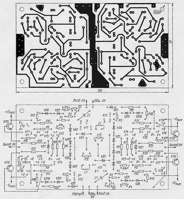
The author treats electronic devices for protection against failure of powerful amplifier transistors with some prejudice due to the complex nature of the load resistance and therefore limited himself to installing 5 A fast-acting fuses located in the power supply in the power circuits for each of the two amplifiers. The rectifiers for each channel of the stereo amplifier must be separate, and the capacitance of the filter capacitors must be at least 10 μF. After adjustment, the following parameters of the amplifier are provided: rated power at a load of 4 Ohms - no less than 70 W, amplified frequency band - 20...20 Hz, harmonic distortion - no more than 000%. The nominal input voltage is about 0,01 V, but by increasing the resistance of resistor R2, the sensitivity of the UMZCH can be increased. The printed circuit board (Fig. 3) is well suited for installation on the heat sink from the Elfa-203-3 reel-to-reel tape recorder; I assembled this stereo amplifier in the casing of this tape recorder.
Transistors VT9, VT10 are installed on a heat sink, which is the rear wall of the case, to which the board is attached. Transistors VT11, VT12 are installed on another heat sink (ready from the Vega 50U-122S amplifier was used). The length of the connecting wires from the board to the terminals of powerful transistors should be minimal. To reduce interference to the inductors, it is useful to place them in shielding cases, for example, from old K50-6 oxide capacitors of the appropriate size. On the board in some places it is necessary to install jumper wires (shown with a dashed line). Debugging the operating mode of the amplifier and adjusting the quiescent current of the output stage should be carried out before installing the board into the device housing. For better “isolation” of the UMZCH channels, the power supply rectifiers are made separate (the secondary windings should also be separate). Fuses included in the power circuit to protect the UMZCH during a load short circuit are installed in the power supply. Literature
Authors: V.Levitsky, Drochia, Moldova, I.Beloborodov, Novosibirsk
Machine for thinning flowers in gardens
02.05.2024 Advanced Infrared Microscope
02.05.2024 Air trap for insects
01.05.2024
▪ Smartphones ZTE Nubia Z5S and Z5S mini ▪ Unexpected properties of yogurt ▪ LCD and plasma: no demand, prices will fall sharply ▪ Rapidly charged quantum battery
▪ site section Power supplies. Article selection ▪ article Weather vane Carlson. Tips for the home master ▪ article Which animals have cube-shaped feces? Detailed answer ▪ article Communication and radio electrician. Job description ▪ article Thyristor timers. Encyclopedia of radio electronics and electrical engineering ▪ article AC detector. Encyclopedia of radio electronics and electrical engineering
Home page | Library | Articles | Website map | Site Reviews
www.diagram.com.ua |


 Leave your comment on this article: