|
|


 Arabic
 Bengali
 Chinese
 English
 French
 German
 Hebrew
 Hindi
Hindi Italian
 Japanese
 Korean
 Malay
Malay Polish
 Portuguese
 Spanish
 Turkish
 Ukrainian
 Vietnamese
|
ENCYCLOPEDIA OF RADIO ELECTRONICS AND ELECTRICAL ENGINEERING A simple broadband RF signal generator. Encyclopedia of radio electronics and electrical engineering
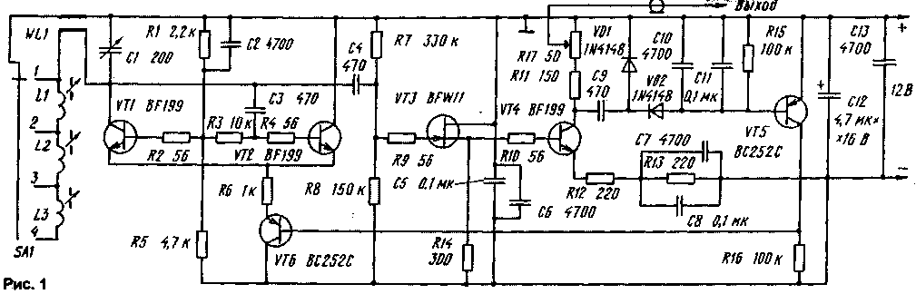
Encyclopedia of radio electronics and electrical engineering / Measuring technology The proposed high-frequency signal generator attracts with its simplicity of design and provides stabilization of the output voltage in a wide frequency band. The requirements for a broadband signal generator are well known. First of all, this is a rather small value of the output impedance, which makes it possible to match its output with the wave impedance of the coaxial cable (usually 50 Ohms), and the presence of automatic adjustment of the output voltage amplitude, which maintains its level almost constant regardless of the change in the frequency of the output signal. For the microwave range (above 30 MHz), simple and reliable switching of ranges, as well as a rational design of the generator, are of great importance. The schematic diagram of the device is shown in fig. 1. Transistors VT1, VT2 together with a variable frequency setting capacitor C1 and inductances L1 - L4 form a master oscillator (frequency range 2 ... 160 MHz). The R1R5 divider sets the DC bias voltage for these transistors. Resistors with a low resistance value are included in the base (gate) circuits of transistors VT1 - VT4; they serve to suppress parasitic generation of high-frequency transistors. By adjusting the current flowing through the common resistor R6 in the emitter circuit of transistors VT1 and VT2, the mode of sinusoidal oscillations with low distortion at a voltage amplitude of several volts can be set.
The high-frequency signal from the generator through the capacitor C4 is fed to the gate of the field-effect transistor VT3. This provides an almost perfect decoupling of the load and the generator. To set the bias voltage of transistors VT3 and VT4, resistors R7, R8 are used, and the current mode of the cascade is determined by resistors R12 - R 14. To increase the degree of decoupling, the output high-frequency voltage is removed from the VT4 collector circuit. To stabilize the level, the RF signal through the capacitor C9 is supplied to the rectifier with voltage doubling, made on the elements VD1, VD2, C10, C11, R15. Proportional to the amplitude of the output signal, the rectified voltage is additionally amplified in the control circuit at VT5 and VT6. In the absence of a signal, the RF transistor VT6 is fully open; in this case, the maximum supply voltage is supplied to the master oscillator. As a result, the conditions for self-excitation of the generator are facilitated and a large amplitude of its oscillations is established at the initial moment. But this RF voltage through the rectifier opens VT5, while the voltage at the base of VT6 increases, which leads to a decrease in the generator supply voltage and, ultimately, to stabilization of the amplitude of its oscillations. The equilibrium state is established when the amplitude of the RF signal on the VT4 collector is slightly higher than 400 mV. The variable resistor R17 (shown as a potentiometer) is in fact an RF attenuator and in the absence of a load at its output, the maximum voltage reaches a quarter of the input, i.e. 100 mV. When the coaxial cable is loaded with a resistance of 50 ohms (which is necessary for its matching in the frequency range from 50 to 160 MHz and higher), an RF voltage of about 50 mV is set at the generator output, which can be reduced to the required level by adjusting the attenuator. A 17-ohm Prech attenuator was used as the R50 regulator in the oscillator circuit. If some specific application does not require adjustment of the output voltage level, the attenuator R17 can be replaced by a fixed 50 ohm resistor. However, even in this case, it remains possible to adjust the RF voltage level within certain limits: for this purpose, the capacitor C9 is connected not to the VT4 collector, but to its emitter, and one has to take into account a slight change (decrease) in the signal level at higher frequencies of the operating range. Then the load for VT4 is formed by the attenuator R17 and resistors R11, R12. An increase in the amplitude of the output high-frequency voltage can be achieved by closing the resistor R11 with a wire jumper, but if it is required to reduce the amplitude of the output voltage, then the resistor R11 is left in the device, and the capacitors C7, C8 are soldered. An even greater decrease in the output signal level can be obtained by reducing the value of the resistance R17, but in this case there will no longer be an agreement with the cable, and at frequencies above 50 MHz this is unacceptable! All parts of the generator are located on a small printed circuit board. The inductors of the generator L1 - L3 are wound on frames with a diameter of 7,5 mm. Their inductances are trimmed with low-loss ferrite cores designed for operation in the VHF band. Coil L3 has 62 turns, L2 - 15 and L1 - 5 turns of PEL 0,2 wire (winding of all coils in one layer). The inductance WL1 is made in the form of a loop, which is attached to the range switch on one side, and to the variable capacitor C1 on the other. The dimensions of the loop are shown in fig. 2. It is made of 1,5mm diameter silver-plated copper wire; to fix the distances between its conductors, three plates of insulating material with low losses (for example, fluoroplastic) are used, in which two holes with a diameter of 1,5 mm are drilled, located respectively at a distance of 10 and 2,5 mm (Fig. 2).
The entire device is placed in a metal case measuring 45x120x75 mm. If the attenuator and the RF connector are installed in the case on the side opposite to that on which the printed circuit board is located, then inside the device case there is still enough space for the power supply units: a 1 W power transformer with a decrease in mains voltage to 15 V, a rectifier bridge and a microcircuit 7812 (domestic analogue - KR142EN8B). A miniature frequency meter with a frequency prescaler can also be placed in the case. In this case, the divider input should be connected to the VT4 collector, and not to the output connector, which will allow the frequency to be read at any RF voltage taken from the R17 attenuator. It is possible to change the frequency range of the device by changing the inductance of the circuit coil or the capacitance of capacitor C1. When expanding the frequency range towards higher frequencies, the losses of the tuning circuit should be reduced (use of a capacitor with an air dielectric and ceramic insulation as C1, inductors with low losses). In addition, the diodes VD1 and VD2 must comply with this extended frequency range, otherwise, with increasing frequency, the output voltage of the generator will increase, which is explained by a decrease in the efficiency of the stabilization circuit. To facilitate tuning, an additional variable capacitor of small capacity (electric vernier) is connected in parallel with C 1, or a mechanical vernier is used to the tuning capacitor with a gear ratio of 1:3 - 1:10. In this design, the BF199 transistors can be replaced by domestic ones - KT339 with any letter index, and when expanding the generator range towards higher frequencies - KT640, KT642, KT643. Instead of the BFW11 field effect transistor, it is permissible to install KP307G or KP312, and instead of the VS252S transistor, KT3107 with indices Zh, I, K or L is suitable. Microwave detector diodes, for example, 2A201, 2A202A, can be used as diodes. If the generator operates at frequencies not exceeding 100 MHz, then diodes of the GD507A type (with correction of the resistance of the resistor R11) can also be used. Switch SA1 - PGK. The power of the resistors is 0,125 or 0,25 watts. Capacitor C1 must be with an air dielectric and have ceramic or quartz insulation of both stator plates from the body and rotor plates from the axis; its maximum capacitance is best limited to 50 pF. Attenuators of the type used in the generator are not produced by our industry. Instead, it is allowed to use a smooth regulator in the auto-regulation circuit and a conventional stepped attenuator with P or T-shaped links at the output. You can also try to make an attenuator with a continuously adjustable output voltage by modifying standard variable resistors for this purpose. Note that the range of adjustment of the output level of self-made attenuators can be significantly increased if they are made on the basis of a sliding variable resistor, to the conducting layer of which, on one side, a narrow metal strip is attached along the entire length. It is connected to a common wire and body. Literature
Publication: N. Bolshakov, rf.atnn.ru
Machine for thinning flowers in gardens
02.05.2024 Advanced Infrared Microscope
02.05.2024 Air trap for insects
01.05.2024
▪ Lethal dose of chocolate calculated ▪ Digital camera with built-in radio ▪ Ultra-budget smartphone Infinix Smart 7 HD
▪ section of the site Car. Article selection ▪ article History of medicine. Lecture notes ▪ article Names of which currencies originated from measures of weight? Detailed answer ▪ article Locksmith of mechanical assembly works. Standard instruction on labor protection ▪ article Remote control of lighting. Encyclopedia of radio electronics and electrical engineering ▪ article Ball in the bag. Focus secret
Home page | Library | Articles | Website map | Site Reviews
www.diagram.com.ua |


 Leave your comment on this article: