|
|


 Arabic
 Bengali
 Chinese
 English
 French
 German
 Hebrew
 Hindi
Hindi Italian
 Japanese
 Korean
 Malay
Malay Polish
 Portuguese
 Spanish
 Turkish
 Ukrainian
 Vietnamese
|
ENCYCLOPEDIA OF RADIO ELECTRONICS AND ELECTRICAL ENGINEERING Pulse-width discriminator. Encyclopedia of radio electronics and electrical engineering
Encyclopedia of radio electronics and electrical engineering / Radio amateur designer The version of the discriminator offered to the attention of readers is designed to demodulate signals with pulse width modulation (PWM). It can be used to demodulate FM signals and in loopback devices where the FM signal is pre-converted to PWM; in pulsed range generators, it can serve to maintain a constant duty cycle in the operating frequency range. The discriminator can be useful in automation devices, allowing you to do without adjusting the device response threshold, since it corresponds to a zero voltage level.
The characteristic of the discriminator is symmetrical with respect to "zero" (Fig. 1), corresponding to the duty cycle Q of the pulses at the input of the discriminator: Q=T/to=2, where T is the pulse repetition period, to is the pulse duration. The linear characteristic is the more, the closer to the rectangular shape of the input signal; with a sinusoidal input signal, it is S-shaped. The degree of curvature of the characteristic also really depends on the frequency of the input signal and the load capacitance. When the pulse duration deviates relative to the value to, the node generates a voltage of positive or negative polarity, depending on the sign of the deviation, proportional to the depth of the deviation.
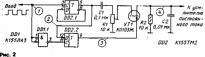
Schematic diagram of the discriminator is shown in Fig.2. The device consists of two frequency dividers by 2, assembled on triggers DD2.1 and DD2.2, and a phase detector on a transistor VT1. The sequence of pulses with PWM is fed directly to the input C of the DD2.1 trigger, and to the input C of the DD2.2 trigger - through the inverter DD1.1. As a result of dividing the frequency of antiphase oscillations at the direct output of both triggers, two sequences of pulses of the "meander" type are formed, shifted one relative to the other in phase. The phase shift is proportional to the pulse duration and is in the range 0 < φ < 180°. Figure 3 shows the voltage diagrams at the characteristic points of the node with the duty cycle of the input pulses Q=2. The diagrams show that the phase shift of the signals in this case is 90°.
From the direct output of the trigger DD2.1 through the decoupling capacitor C1, which eliminates the constant component from the signal spectrum, the voltage is fed to the input of the phase detector - to the drain of the field effect transistor VT1. Trimmer resistor R1 is used to set the level of the input signal so that it does not exceed the upper limit of the dynamic range of the demodulator. Otherwise, the asymmetry of its characteristic occurs due to the effect of direct detection of the input signal on the non-linearity of the transistor channel. The gate of the transistor receives pulses from the direct output of the trigger DD2.2, ensuring the operation of the transistor in the key mode. The R2C2 filter selects the direct component of the output voltage, proportional to f, which is then fed to the input of the DC amplifier. Diagram 4 in Fig. 3 shows the form of the output voltage of the node when the capacitor C2 is off. Obviously, with the duty cycle of the input pulses Q=2, the constant component of the voltage is zero. The filter time constant is chosen based on the specific application of the discriminator. The diagram shows the values of the filter elements for the case of using the discriminator as a demodulator of FM signals with the following parameters: fо==500 kHz, f=12 kHz, O=4 kHz. With a voltage at the input of the phase detector of 0,5 V, the slope of the characteristic is approximately 0,2 mV / kHz, so an amplifier is needed at the output of the detector. Resistors and capacitors used in the node can be of any type. The field effect transistor is selected with a cut-off voltage of not more than 3,5 V. Setting up the discriminator comes down to setting a voltage level at the input of the phase detector that does not cause a "zero" shift in the characteristic. By applying a "meander" signal to the input of the node, the trimming resistor R1 sets zero voltage at the output of the DC amplifier. A change in the duty cycle of the pulses in this case should be accompanied by a symmetrical deviation of the voltage in both directions relative to "zero". Author: A. Rudnev, Balashov, Saratov region; Publication: N. Bolshakov, rf.atnn.ru
A New Way to Control and Manipulate Optical Signals
05.05.2024 Primium Seneca keyboard
05.05.2024 The world's tallest astronomical observatory opened
04.05.2024
▪ Global Shutter CMOS image sensor with extended dynamic range ▪ Solar panels LG NeON R and NeON R Prime ▪ Warm nanoparticles stimulate the brain ▪ Graphene electric generator on fluctuations in ambient temperature
▪ section of the site Fundamentals of safe life (OBZhD). Article selection ▪ article by Henri de Regnier. Famous aphorisms ▪ article Why is the Hatter from Alice in Wonderland insane? Detailed answer ▪ Article Head of Supply Department. Job description ▪ article Special enamels. Simple recipes and tips ▪ article Generator to power the LED. Encyclopedia of radio electronics and electrical engineering
Home page | Library | Articles | Website map | Site Reviews
www.diagram.com.ua |


 Leave your comment on this article: