|
|


 Arabic
 Bengali
 Chinese
 English
 French
 German
 Hebrew
 Hindi
Hindi Italian
 Japanese
 Korean
 Malay
Malay Polish
 Portuguese
 Spanish
 Turkish
 Ukrainian
 Vietnamese
|
ENCYCLOPEDIA OF RADIO ELECTRONICS AND ELECTRICAL ENGINEERING Decoder for a simple telecontrol system. Encyclopedia of radio electronics and electrical engineering
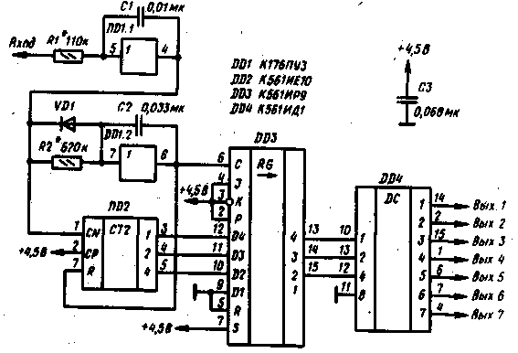
Encyclopedia of radio electronics and electrical engineering / Radio control equipment The encoder scheme is described in the article "Telecontrol encoder and decoder". The decoder circuit is shown in Fig.1. Packets of input pulses of negative polarity are fed to the shaper, assembled on the elements R1, C1, DD1.1. Such a shaper has the properties of an integrating circuit and a Schmitt trigger. At its output, the pulses are somewhat delayed relative to the input ones and have steep fronts, regardless of the steepness of the fronts of the input pulses, in addition, this shaper suppresses impulse noise of short duration.
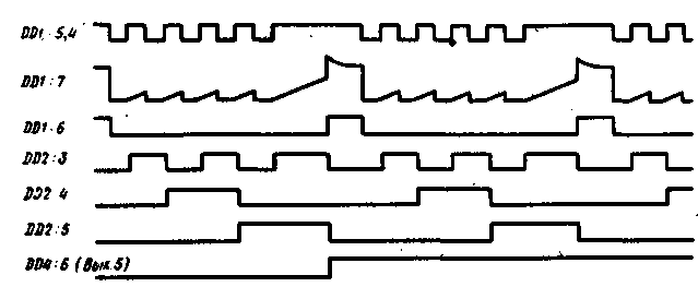
From the output of the element DD1.1, the pulses are fed to the pause detector. It is assembled on the elements R2, C2, VD1, DD1.2. The operation of the pause detector is illustrated in Fig. 2 (diagrams DD1:7 and DD1:6).
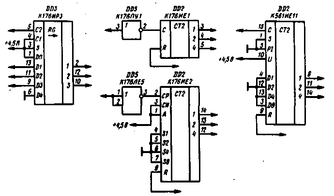
The first negative pulse of the pack, passing through the diode VD1 to the input of the element DD1.2, switches it to state 6. In the pause between the pulses, the capacitor C2 is gradually charged by the current flowing through the resistor R2, while the voltage, however, does not reach the switching threshold of this element. Each subsequent input pulse through the diode VD1 quickly discharges the capacitor C2, so during the operation of the pack at the output DD1.2 log.0. In the pause between bursts, the voltage at the input of the DD1.2 element reaches the switching threshold, this element switches like an avalanche (due to positive feedback through the capacitor C2) to state 1. As a result, in the pause between bursts, a positive pulse is formed at the output 8 of the DO 1.2 element, resetting counter DD2 to 0. The pulses from the output of the shaper DD1.1 are also fed to the counting input CN of the counter DD2, as a result of which, after the end of the pack, the counter is set to a state corresponding to the number of pulses in the pack. The front of the pulse from the pause detector DD1.2 rewrites the state of the counter in the register DD3. The output signals of the DD3 register are fed to the DD4 decoder, as a result, when receiving bursts of one to seven pulses, a log.4 appears at the corresponding output of the DD1 decoder. After receiving a burst of eight pulses, log.1 appears at the output O of the decoder DD4, it is not used. The described encoder is assembled on a printed circuit board made of fiberglass with a thickness of 1 mm. The dimensions of the double-sided decoder board are 42,5x45 mm, the drawings are shown respectively in Fig.3. The devices used resistors MLT-0,125, capacitors KM-5 and KM-6. Without processing printed circuit boards, instead of microcircuits K561IE8, K561LE10 and K561ID1, the corresponding microcircuits of the K176 series can be used, however, not all of them can work normally at a supply voltage of 4,5 V, it may be necessary to increase it to 9 V. If the K176PUZ microcircuit is replaced by K561PU4 ( this replacement is also possible without changing the PCB pattern), the supply voltage can be selected in the range of 3...15 V. The K561IE10 (KR1561IE10) chip in the decoder can be replaced with K561IE11, K176IE1, K176IE2, the K561IR9 chip is replaced with K176IRZ, however, these replacements require processing of circuits and printed circuit boards (Fig. 4). In addition, non-inverting elements of the K176PUZ microcircuit can be replaced with elements of other microcircuits, as described in the second section of the book. The K561IE8 chip can be replaced with the K561IE9, in which case the number of commands will be reduced to five.
It is recommended to assemble the system and configure it in the following sequence. On the encoder board, by selecting resistors R 1 and R2, set the pulse frequency to 180 ... 220 Hz with a duty cycle close to 2. In the absence of an oscilloscope, you can use a high-resistance DC voltmeter - the average voltage at pin 9 DD1.2 should be equal to half or be several less than half the supply voltage. The exact value of the frequency does not play a special role, and the duty cycle should be maintained. Then you can check the correctness of the generation of packs by pressing the buttons SB1-SB7 in turn. At the same time, at the output 10 DD1.3 there should be packs of 1-7 pulses, if the buttons are not pressed, the number of pulses in packs should be 8. In the absence of an oscilloscope, the correct generation of packs can be judged by the average voltage at the output of DD1.3 - when in packs of eight pulses, it should be 40% of the power supply voltage, with seven pulses - 39%, with six - 37,5%, with five - 36%, with four - 33%, with three - 30%, with two - 25%, with one impulse in a pack-17%. Then you need to assemble the decoder and connect the output of the encoder and the input of the decoder. In the decoder, you should make sure that the pulses pass through the DD1.1 shaper, their shape and duty cycle should not noticeably change, and that the pause detector is working correctly - the duration of the positive pulses at pin 6 of the DD1.2 element should be about the period of the input pulses, the average voltage at this output in the absence of command transmission (i.e., when bursts of eight pulses are applied) should be about 10% of the supply voltage, when the SB1 button is pressed - 33%. If necessary, set the duration of the specified pulse by selecting R2. Further, when forming bursts of one to seven pulses in the encoder, you should make sure that, at the same time, potential signals with a log level appear at the corresponding input of the decoder chip DD4 and at its outputs. 1. For reliability, it is advisable to repeat the last check by increasing and decreasing the capacitance of the encoder capacitor C1 by 20%, for which a 1300 pF capacitor is installed in parallel with it, then 0,033 μF in series. Such a check ensures that the device remains operational with fluctuations in temperature and supply voltage. Literature 1. S.A. Biryukov. Digital devices based on MOS integrated circuits. M. Radio and communication. 1996 Publication: N. Bolshakov, rf.atnn.ru
The world's tallest astronomical observatory opened
04.05.2024 Controlling objects using air currents
04.05.2024 Purebred dogs get sick no more often than purebred dogs
03.05.2024
▪ The Digital Key standard will turn your smartphone into a car key ▪ Refractory clay supercapacitor
▪ section of the site Biographies of great scientists. Article selection ▪ article Converter. History of invention and production ▪ article Where do they show their tongues to each other? Detailed answer ▪ article Shikhtovchik. Standard instruction on labor protection ▪ article Grounding system TN-C. Encyclopedia of radio electronics and electrical engineering ▪ article Money doesn't burn. Focus secret
Home page | Library | Articles | Website map | Site Reviews
www.diagram.com.ua |

 Leave your comment on this article: