|
|


 Arabic
 Bengali
 Chinese
 English
 French
 German
 Hebrew
 Hindi
Hindi Italian
 Japanese
 Korean
 Malay
Malay Polish
 Portuguese
 Spanish
 Turkish
 Ukrainian
 Vietnamese
|
ENCYCLOPEDIA OF RADIO ELECTRONICS AND ELECTRICAL ENGINEERING Digital reverb. Encyclopedia of radio electronics and electrical engineering
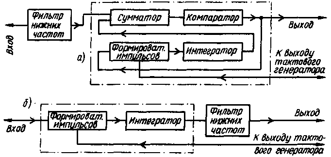
Encyclopedia of radio electronics and electrical engineering / Digital technology In recent years, thanks to the emergence of the necessary element base, it has become possible to implement the reverberation effect electronically, which makes it possible to significantly improve the quality and performance characteristics of the reverb, reduce its dimensions and power consumption. As you know, a reverb is a device for delaying an analog audio signal. In electronic reverberators, the functions of the delay line are performed by an N-bit shift register, the input of which is fed the digital equivalent of the input analog signal converted by the analog-to-digital converter (ADC), and the analog converter (DAC) is connected to the output, restoring again the analog signal from the digital equivalent. The ADC output code can be either parallel or serial. With a parallel code, it is necessary to provide for a delay in the signals of each bit, which leads to an increase in the number of shift registers by K times, where K is the number of ADC bits. With serial code, the delay line is performed on one shift register, however, at its output, it is necessary to turn on the serial-to-parallel converter if the output DAC processes the parallel count. The delay time in the first case will be determined by the ratio of the number of bits of the shift register to the clock frequency, and in the second - by the product of the number of bits of the register by the time of formation of the K-bit serial code. Both of these methods are relatively difficult to implement, since a relatively large number of bits of digital codes is required to obtain a good quality of the delayed signal, and this requires the use of complex ADCs, DACs, and high-order low-pass filters at the input and output of the device. A simpler way to obtain a digital sequence from an analog signal that can be delayed by a shift register is delta modulation, which allows you to digitize not the current value of the signal, but its change relative to the previous one. The block diagram of the delta modulator is shown in fig. 1, a. The LPF limits the spectrum of the input analog signal before it is applied to the input of the modulator. The adder generates the difference of two signals: input and restored output. Depending on the sign of the instantaneous value of this difference, the comparator outputs either a logical level of 0 or 1, i.e., the output signal of the modulator is a sequence of pulses with variable duration and duty cycle. To apply to the input of the adder, this sequence is passed through a recovery channel containing a pulse shaper and an integrator.
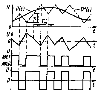
The demodulator (Fig. 1b) is essentially an analogue of the modulator recovery channel. An important feature of the delta modulator - demodulator system is the mandatory identity of the recovery channels. On fig. Figure 2 shows a simplified form of the signals at characteristic points of the modulator: A - input signal u(t) and reconstructed u*(t) supplied to the adder, B - difference output signal of the adder, C - signal from the output of the comparator, G - signal, at the input of the integrator. From fig. 2 shows that in order to improve the approximation of the input signal, it is necessary to increase the clock frequency. However, in a reverb, for the same delay time, this would require an increase in the "length" of the shift register connected between the modulator and demodulator, as well as the use of faster elements.
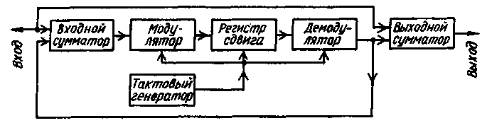
At the same time, the analysis shows that better approximation can be achieved without changing the clock frequency. It is only necessary, depending on the steepness of the signal curve at some point (and, hence, on the width of its spectrum), to change the value of D accordingly, i.e., to change the steepness of the approximating signal. You can change A by changing either the constant of integration of the integrator, or the amplitude of the pulses supplied to it. The reverb described below uses a change in the integration constant. As a variable resistor, a field-effect transistor is used, controlled by a voltage coming from a passive integrating circuit, to which a signal is applied from the EXCLUSIVE OR element. In other words, the delta modulator converts not the signal itself into a digital sequence, but its derivative, from which the original signal can be restored by integrating at the output. About delta modulation and its application can be found in [I, 2, 3]. The digital reverb described below is based on the principle of adaptive delta modulation and can be used both as an EMI and EMC functional unit, and as an independent device for implementing reverberation and echo effects in amateur ensembles. It is also interesting to use it in a household radio complex to simulate a large room. The block diagram of the reverb is shown in Fig.3. The input adder adds the input signal to the delayed part, which allows you to get the effect of multiple sound reflections. The modulator converts it into a digital sequence, which the M-bit shift register delays for a time Tz. This time, and hence the reverberation (echo) time, can be determined by the formula: Тз=N/4, where fi is the clock frequency. The demodulator reconstructs the original analog signal from the digital sequence.
The output adder serves to add the delayed signal to the input, and the level of the delayed signal can be adjusted, which allows you to smoothly change the reverb depth from zero to maximum. Main technical characteristics.
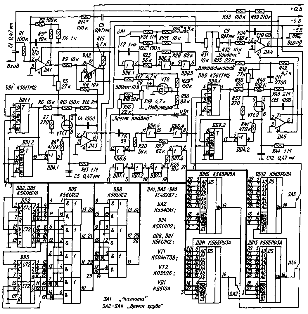
The circuit diagram of the reverb is shown in fig. 4. The input adder is made on the op-amp DA1, which simultaneously performs the functions of a first-order low-pass filter that limits the spectrum of the total signal.
The modulator includes microcircuits DA2, DA3, DD1, logic element DD4.1 and field effect transistor VT1.1. The modulator works as follows. Comparator DA2 compares the voltage of the signal coming from the output of the adder with the voltage at the DA3 integrator and, depending on which one is greater, generates a signal of 0 or 1, respectively. This signal is fed to the information input of the trigger DD1.1, which performs the functions of a digital sample-and-hold device. The pulse sequence from the trigger output is transmitted to the input of the shift register and to the device for converting unipolar pulses into symmetrical bipolar ones, made on resistors R5-R7. Pulse symmetries are achieved with a trimming resistor R5. Next, the pulses are fed to the integrator, the integration constant of which is changed by means of a field-effect transistor VT1.1, controlled by a signal from the element DD4.1. The field effect transistor VT1.1, the element DD4.1 and the triggers of the DD1 chip make up the adaptation node. This node changes the integration constant, and hence the slope of the integrator output signal, depending on the amplitude and frequency of the input signal, which allows you to get a linear frequency response in a wide frequency band with a good signal-to-noise ratio. If in the digital sequence in adjacent cycles the logical levels are different, which corresponds to a small change in the input signal, then level 4.1 is formed at the output of the "EXCLUSIVE OR" element DD1. This leads to an increase in the voltage at the gate of the field-effect transistor VT1.1 and an increase in the resistance of its channel . As a result, the time constant of the integrator will increase and, accordingly, the slope of its output voltage will decrease. With a strong change in the input signal, the slope of the voltage at the output of the integrator will increase accordingly. The shift register is made on microcircuits DD10-DD13. which are dynamic RAM with a capacity of 16 K with the organization in one bit. Microcircuits DD2, DD3 perform the functions of an address counter, and microcircuits DD5, DD8 .- switch the address of the rows and addresses of the columns of the RAM. It turned out to be possible to abandon the regeneration device, since at a clock frequency of 100 kHz, the rotation time for all RAM rows is less than 2 ms. The demodulator assembled on the op-amp DA5, two flip-flops DD9.1 and DD9.2 and a field-effect transistor VT1.2 must be identical to the modulator (if the comparator is conditionally removed from it). The op-amp DA4 has an output adder, which, like the input adder, simultaneously performs the functions of a first-order low-pass filter. Variable resistor R31 allows you to change the duration (depth) of the reverberation, and R32 - the level of the delayed signal. The clock generator is assembled on the elements DD6.4-DD6.6 according to the integrator-comparator circuit, the frequency of which can be smoothly changed by a variable resistor R16, which leads to a smooth change in the delay time (reverberation time). On the elements DD6.1-DD6.3 and the transistor VT2, a generator of sinusoidal oscillations of an infrasonic frequency is assembled, which allows modulating the frequency of the clock generator when implementing the "chorus" effect. Switch SA1 is used to step change the frequency of the generator. The modulation depth is set by a variable resistor R19. Setting up a reverb begins with checking the operation of the clock generator. Connect the input of the oscilloscope to the output of the DD6.4 element and observe rectangular pulses on the screen, the duration of which should be approximately 1 μs, and the repetition frequency should be changed by the variable resistor R16 (when the variable resistor R19 slider is set to the lower position according to the circuit) from 100 to 500 kHz. In the generator of sinusoidal oscillations, a selection of resistors R24 and R29 achieve a sinusoidal waveform (the input of the oscilloscope is connected to the negative plate of capacitor C8). After checking the operability of the clock generator and the generator of sinusoidal oscillations, they begin to establish the modulator. Its input is connected to a common wire, and an oscilloscope is connected to the output of the op-amp DA3. Triangular-shaped pulses are observed on the screen, the symmetry of which is set with a tuning resistor R5. Amplitude of impulses. should be no more than 5 mV, and the frequency is two times less than the clock. After the performed operations, the input of the modulator is disconnected from the common wire and connected to the output of the input adder, to the input of which a signal with an amplitude of 140 mV and a frequency of 20 Hz is supplied from the sound generator. At the output of the op amp DA3 there should be a signal of the same frequency, but with an amplitude 10 times greater, and shifted by 180 ° relative to the input. By changing the frequency of the input signal from 20 Hz to 14 kHz, the linearity of the frequency response of the modulator is achieved by selecting the resistor R8. The demodulator is adjusted in the same order as the modulator. First, the D-input of the trigger DD9.1 is disconnected from the switch SA3 and connected to the direct output of the trigger DDI.I. The input of the reverb is connected to a common wire, an oscilloscope is connected to the output of the op-amp DA5 and a trimming resistor R38 balances the triangular signal. Then a signal with an amplitude of 140 mV and a frequency of 20 Hz to 14 kHz is supplied from the sound generator, and by selecting the resistor R41, the parameters of the modulator and demodulator are identical. After that, the D-input of the trigger DD9.1 is again connected to the switch SA3. The signal at the output of the demodulator must be delayed relative to the input, which is checked (at the minimum clock frequency) by quickly removing the signal from the input of the reverb. At the output, the signal should disappear after a certain time equal to the delay time. The output adder has no features and, as a rule, starts working immediately. A selection of resistor R14 sets the maximum reverberation time (number of echo repetitions) at the upper position of the variable resistor R3 slider according to the scheme). Selecting the resistor R34, set the maximum level of the delayed signal in the output. To power the reverb, you need a low-power stabilized source with output voltages of 12 V and 2X5 V. The current consumed from each source does not exceed 30 mA. To eliminate interference, it is necessary to shunt the lithium lines with oxide capacitors with a capacity of at least 10 μF with ceramic capacitances of 0,1 μF connected in parallel. Near each positive output of the DD10-DD13 microcircuits, shunt ceramic capacitors with a capacity of 0,22 microfarads must also be included. Trimmer resistors used in the device - SP5-3, variables - SP-1. Capacitors: ceramic - KM-5 and KM-6, oxide - K50-6. Instead of OU K140UD7, K140UD6, K544UD1, K140UD8 can be used. The comparator K554CA1 can be replaced by K554CA2, K554CAZ, K521CA1-K52ICA3, taking into account the features of their inclusion. Chips of the K561 series can be replaced by the corresponding ones from the K164 or K176 series. When developing the reverb, the goal was to create the simplest possible device with relatively high values of quality and performance. Further improvement in quality can be achieved by using more complex adaptation nodes in the modulator and demodulator. Reducing the amount of memory due to a stepwise decrease in the "length" of the address counter (for example, by introducing a 14-position switch, the general direction output of which is connected to the combined R-inputs of the DD2, DD3 microcircuits, the position outputs to the counter bits) will make it possible to sequentially switch from the echo effect "to reverb," flanger "," phaser "and so on until the delay is completely eliminated. But all this leads to a complication of the circuit, which an experienced radio amateur may well implement on his own if he wishes. Literature: 1. Venediktov M. D., Zhenevsky Yu. P., Markov V. V., Eidus G. S. Delta modulation. Theory and application. - M.: Communication. 1976.
Author: V. Barchukov, Moscow; Publication: N. Bolshakov, rf.atnn.ru
Artificial leather for touch emulation
15.04.2024 Petgugu Global cat litter
15.04.2024 The attractiveness of caring men
14.04.2024
▪ Magnetic monopoles in a cold quantum gas medium ▪ Xerox DocuMate 4700 Flatbed Scanner for SMB ▪ Sound can travel even in a vacuum ▪ Drones are controlled by gestures
▪ section of the site Aphorisms of famous people. Article selection ▪ article Vale of weeping. Popular expression ▪ article Working with solvents. Standard instruction on labor protection ▪ article Unusual envelope. Focus secret
Comments on the article: Alex Collected 25 years ago! It still works! Only the signal-to-noise ratio is not very good.
Home page | Library | Articles | Website map | Site Reviews
www.diagram.com.ua |

 Leave your comment on this article: