|
|


 Arabic
 Bengali
 Chinese
 English
 French
 German
 Hebrew
 Hindi
Hindi Italian
 Japanese
 Korean
 Malay
Malay Polish
 Portuguese
 Spanish
 Turkish
 Ukrainian
 Vietnamese
|
ENCYCLOPEDIA OF RADIO ELECTRONICS AND ELECTRICAL ENGINEERING Paging receiver for 148...174 MHz range. Encyclopedia of radio electronics and electrical engineering
Encyclopedia of radio electronics and electrical engineering / radio reception The paging system is designed to organize dispatch networks in organizations, industrial enterprises, construction, residential areas, etc. The system provides for: prompt notification of personnel within the service area; individual call to 100 thousand subscribers and transmission of alphanumeric information to them (for example, the phone number to call) displayed on the 8-digit alphanumeric LCD indicator of the wearable receiver; audible call signaling; remembering the last received message; transmission of voice messages. The system contains a stationary transmitter with an AFU, a dispatcher's control panel based on a personal computer, wearable receivers, chargers for wearable receivers. The paging receiver shown in Figure 1 is designed to operate at 150,741 MHz. The presence in the receiver of an 8-bit digital-character indicator on liquid crystals makes it possible to create on its basis radio calling systems of various configurations, coverage, and informativeness [1]. The constructive and circuitry solutions of the receiver are highly flexible and can be easily adapted to the requirements of the consumer. The receiver consists of two rather independent parts - a radio receiver and a decoding device. The radio receiver is made on 9 transistors VT1 ... VT9 and one chip D1 according to a superheterodyne circuit with double frequency conversion and the use of a single-quartz local oscillator.
Consider the operation of the radio receiver. The signal received on the built-in antenna WA1, through the antenna circuit LI, C2, C3, is fed to the input of a single-circuit high-frequency amplifier, made on the transistor VT3, inductance L2 and capacitors C7, C8, C9. The first mixer (transistor VT4) mixes the signal (Fc) taken from the UHF circuit and the signal from the output of the frequency doubler. The multiplier, assembled on the transistor VT5, inductances L3, L4 and capacitors C10 ... C13, doubles the frequency (Fg) of the crystal oscillator (VT6, BQ1). The load of the first mixer is a double-circuit filter L5, L6, C15 ... C18, C21, C22, tuned to the difference frequency Fcv \u2d Fc-8Fg, from the output of which the converted signal is fed through the buffer stage on the VT1 transistor to the input of the DAXNUMX microcircuit. The DA1 chip (K174XA26) is a universal economical path for processing FM signals with a low intermediate frequency and in this case performs the functions of a second frequency mixer, a limiting amplifier and a frequency demodulator. The second mixer is balanced, it converts the RPCH signal into the RPCH frequency, for which one of its inputs (pin 18) receives a RPCH signal, and the second input (pin 1) receives a signal from a crystal oscillator. The difference frequency Pfn=465 kHz is selected by the piezoceramic filter Z1, amplified and detected. The circuit L8, C28, R25 acts as a phase-shifting frequency demodulator circuit. A driver is assembled on the transistor VT9, which converts the output low-frequency signal of the DA1 microcircuit into a sequence of rectangular pulses. The threshold of the shaper is adjusted by potentiometer R27. Due to the presence of a voltage regulator made on transistors VT1, VT2, the radio receiver remains operational when the supply voltage drops to 4V. In the radio receiver, the barrier mode of operation of transistor stages [2] is widely used, the essence of which is the series supply of active elements, which can significantly save current consumption compared to traditional parallel supply. All elements of the radio receiver, together with the built-in antenna, are placed on a printed circuit board measuring 75 x 50 mm. The main characteristics of the radio receiver are given in table.1. Table 1
Table 2
At the input of the decoder, made on the matrix LSI KR1806XM1-584 [3], from the output of the LF radio receiver, a message is received in the form shown in Table 2. The first codegram contains the address, and the second and third contain information.
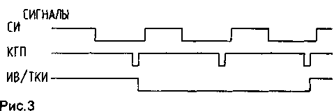
The decoding device of the paging receiver, the electrical circuit of which is shown in Fig. 2, is made on 9 microcircuits. In the initial state, the decoder is in the mode of receiving call pulses (PV). If the address contained in the first codegram coincides with the address wired at the inputs AD1 ... AD24, the CGP signal turns on the sound signaling of the call (D2.2, D2.3, D6.2, HA1) and the D3 decoder is switched to the TKI reception mode . The received first half of the information (the second codegram) is decoded, and the second CGP signal starts the scheme for sequential recording of information in the consumer register (D1.3, D1.4, D4.4, D6.3, D6.4, D7). Information circuit: pin 33 of the D3 chip - pin 3 of the D9 chip. The consumer register is located in a specialized indicator control chip D9 (MBIS K1515XM1-560). The second half of the information is received in the third codegram and is written to the consumer's register in the same way as the first half of the information. The counter (D5.2, D8.1, D8.2) allows writing information to the consumer register and prohibits writing the address when the message is repeated. Figure 3 shows the timing diagrams of some signals.
Eight-digit digital-character indicator HL1 allows you to display any number in the range from 00000000 to 99999999 and any (one of eight) mnemonic character. After viewing the received information, pressing the RESET button (SB1) erases the information that was in the consumer register (D9) and the D3 decoder is switched to the original IW reception mode. The reference clock generator is made on Dl.1, D1.2 microcircuits and a BQ1 quartz resonator. The decoding device, together with the indicator, is placed on a 75 x 50 mm printed circuit board. The overall dimensions of the paging receiver do not exceed 120 x 57 x 24 mm. Literature 1. Tulyakov Yu.M. Personal radio call systems. - M.: Radio and communication, 1988.
Publication: N. Bolshakov, rf.atnn.ru
Artificial leather for touch emulation
15.04.2024 Petgugu Global cat litter
15.04.2024 The attractiveness of caring men
14.04.2024
▪ Antibiotics speed up bacterial growth ▪ Microsoft Surface 2 and Microsoft Surface Pro 2 tablets ▪ Casio XJ-UT310WN Ultra Short Throw Projector ▪ Ocean heat waves threaten marine life ▪ IKEA DIRIGER smart home control center
▪ section of the site Tools and mechanisms for agriculture. Article selection ▪ article It's more than a crime: it's a mistake. Popular expression ▪ article What is the difference between a catapult and a ballista? Detailed answer ▪ article Lake Titicaca. Nature miracle ▪ article Automatic lighting switch. Encyclopedia of radio electronics and electrical engineering
Home page | Library | Articles | Website map | Site Reviews
www.diagram.com.ua | |||||||||||||||||||||||||||||||||||


 Leave your comment on this article: