|
|


 Arabic
 Bengali
 Chinese
 English
 French
 German
 Hebrew
 Hindi
Hindi Italian
 Japanese
 Korean
 Malay
Malay Polish
 Portuguese
 Spanish
 Turkish
 Ukrainian
 Vietnamese
|
ENCYCLOPEDIA OF RADIO ELECTRONICS AND ELECTRICAL ENGINEERING Powerful switching DC voltage regulator. Encyclopedia of radio electronics and electrical engineering
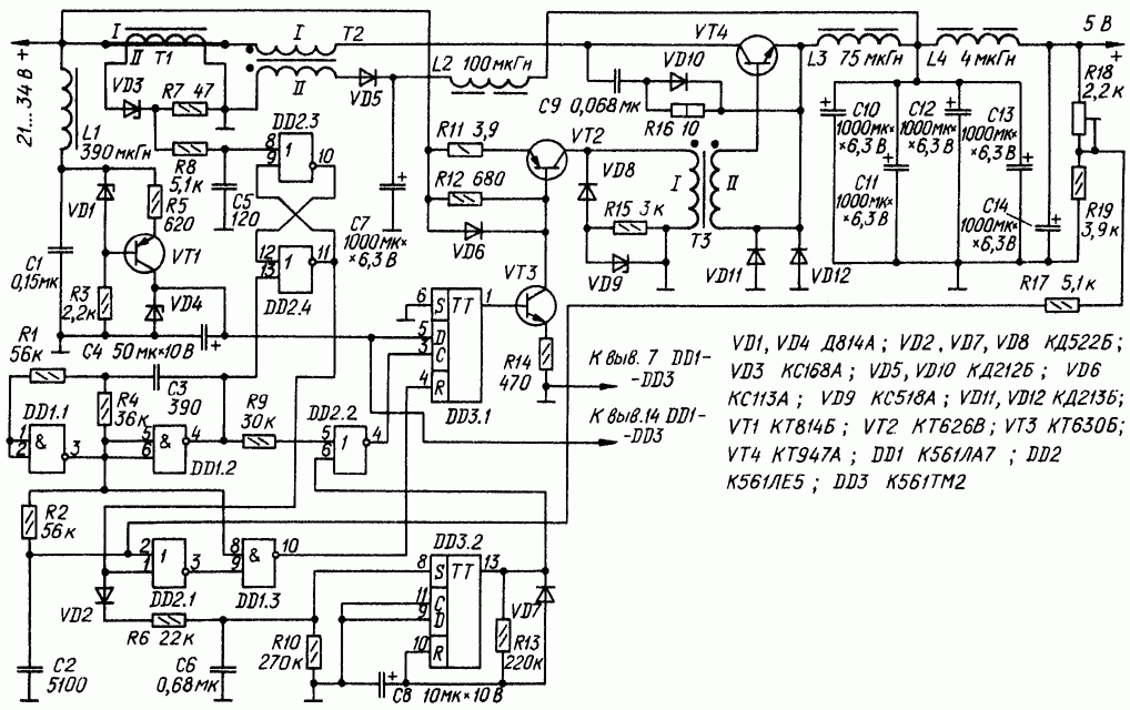
Encyclopedia of radio electronics and electrical engineering / Surge Protectors Among the switching voltage stabilizers, a special class is formed by devices with a pulse-width (PW) principle of output voltage regulation. Their distinctive property is the constancy of the ripple level throughout the entire range of the load current. It is possible to synchronize the stabilizer with powered digital devices, which in some cases makes it possible to simplify the solution of the issue of their compatibility. The stabilizer is designed to power electronic equipment made on digital microcircuits. It has a soft start without output voltage surges, two-stage protection for load current with automatic return to operating mode after overload removal and is able to stay in the output circuit closing mode for a long time. Schematic diagram of the stabilizer is shown in Fig. 1
On the elements DD1.1, DD1.2 made a clock generator of rectangular pulses. The circuit, consisting of resistor R9 and the input capacitance of the element DD2.2, creates some time delay of the pulses. Thus, at the output of the DD2.2 element, a rectangular signal acts, delayed relative to the signal at the output of the DD1.1 element by 0,4 ... 0,5 μs. The pulse-width control node is built on the elements DD1.3, DD2.1, DD2.2 and the trigger DD3.1. The control pulses of the key element of the stabilizer are generated by the trigger DD3.1. On the edge of the delayed pulse of the generator, the trigger switches to a single state. The R2C2 circuit generates triangular voltage pulses with an amplitude of about 2.1 mV at the top input of the DD100 element according to the circuit. The flip-flop switches to state 0 on input R. At startup, the output voltage at the first moment is zero and at the input (pin 2) of the DD2.1 element, only triangular pulses operate, the amplitude of which is less than the threshold voltage of the element (for the CMOS microcircuits used in the stabilizer, it is 0,55 ... 0,6 of their supply voltages). At the lower input of the element DD1.3 there is a single signal and the trigger DD3.1 switches to the zero state when a low level signal appears at the output of the element DD1.1. In this case, the duration of a single state of the trigger DD3.1 is maximum and close to the half-cycle of the generator oscillations, which corresponds to the maximum time of the open state of the key element. When the output voltage reaches the control zone, the voltage at the upper input of the DD2.1 element will have time to increase to the threshold value before the pulse decay appears at the upper input of the DD1.3 element, and the duration of the single state of the trigger DD3.1 decreases to the value in the steady state. From this moment, the increase in output voltage stops - the device goes into stabilization mode. If for some reason (for example, in a sharp decrease in load current) the output voltage increases, then the single trigger output pulse becomes even shorter and the output voltage of the stabilizer again approaches its steady value. The output of the SHI control unit is connected to the input of a pulse amplifier based on transistors VT2, VT3, which is a controlled stable current generator with a transformer output. The current through the secondary winding of the transformer T3 is determined by the resistance of the resistor R11 and is approximately 1,5 A. Controlling the key transistor VT4 from the current generator allows you to force the processes of its switching and obtain a low saturation voltage. With a single state of the trigger DD3.1, the current generator provides a constant current through the primary winding of the transformer T3 during the output pulse of the control unit. A linearly increasing component of the magnetizing current appears in the primary winding. The inductance of the primary winding of the transformer T3 is chosen such that the maximum value of the magnetizing current does not exceed 10 ... 15% of the collector current of the transistor VT2. Thus, the base current of the transistor VT4, while it is open, remains practically unchanged. After the transistor VT2 closes, the transformer T3 is disconnected from the power source and the magnetizing current component begins to decrease, flowing through the VD8VD9R15 circuit. This leads to a change in the polarity of the voltage on both windings of the transformer. The supply of a negative voltage to the emitter junction of the transistor VT4 ensures its forced closing. Technical specifications
When the transistor VT4 is closed, the difference between the input and output voltage is applied to the inductor L3, and the current through it increases. After closing the transistor VT4, the current in the inductor cannot be interrupted instantly, therefore, the diodes VD11, VD12 open, forming a circuit for the current to flow. At the specified value of the inductance, the amplitude. the variable component of the inductor current (and, consequently, the capacitors C10-C13 of the filter) is 3 A at an average current value of up to 15 A. In order to reduce the output voltage ripple, it is necessary to collect the filter by connecting several capacitors in parallel. For better smoothing, an additional filter L4C14 is installed, which reduces the amplitude of the ripple by 3...5 times and prevents the penetration of high-frequency interference into the load. To reduce dynamic losses in the VT4 transistor when it is switched, additional elements T2, VD5, C7, L2 and the C9R16VD10 circuit are introduced into the device. In each period of operation of the device, when the transistor VT4 is opened, its saturation voltage reaches its steady state value in a few tens of nanoseconds. The VD10 diode is closed and does not affect the rate of decrease in this voltage. The collector current of the transistor VT4 increases at a rate determined by the inductance of the primary winding of the transformer T2 and reaches a value of 12 ... 15 A in about 2 μs. Thus, an increase in the collector current of the transistor VT4 occurs at a low value of its saturation voltage, which sharply reduces the dynamic losses in the transistor when it is opened. After the specified time has elapsed, the magnetic circuit of the transformer T2 is saturated, the voltage on its windings decreases to zero, and until the end of the period it does not affect the operation of the stabilizer. When the transistor VT4 is closed, the voltage on the windings of the transformer T2 changes sign, the diode VD5 opens and the energy stored in the transformer is converted into the charge of the capacitor C7. At the same time, the voltage between the collector and emitter of the transistor VT4 begins to increase, the VD10 diode opens, connecting capacitor C9 in parallel with this transistor. Now the rate of voltage increase on the transistor determines the capacitance of the capacitor C9 (the increase time is about 1 μs). The next time transistor VT4 is opened, this capacitor is discharged through resistor R16. the main link of the protection system is the load current sensor, made on the current transformer T1. With a single signal of the clock generator, the trigger of the protection device, assembled on the elements DD2.3, DD2.4, is reset to zero (level 0 at the output of the element DD2.4). At this time, the transistor VT4 is closed. When it is opened, a linearly increasing voltage is supplied to the upper input of the DD2.3 element. When the load current is less than the maximum value, the voltage at the upper input of the element DD2.3 does not exceed the threshold. In the event of an overload, the collector current of the transistor VT4 reaches a value at which the voltage at the upper input of the DD2.3 element exceeds its threshold value and the protection trigger switches to a single state (level 1 at the output of the DD2.4 element). In this case, the trigger DD3.1 is set to the zero state and the transistor VT4 closes. The stabilizer enters the load current limiting mode, its output voltage decreases. This mode is not dangerous for the stabilizer (the collector current of the VT4 transistor is limited), but may be unacceptable for the load. In order to secure the load, the second stage of the protection system is switched on, consisting of an integrating circuit VD2R6R10C6 and a single vibrator on a DD3.2 trigger. The initial state of the trigger DD3.2 - zero. If the overload continues for more than 70 ... 150 ms (depending on its multiplicity), the voltage across the capacitor C6, increasing, reaches the threshold value and the trigger DD3.2 switches to a single state for about 2 s. A single state at the lower input of the element DD2.2 prohibits the supply of clock pulses to the trigger DD3.1 and the stabilizer is turned off. During this time, the capacitor C6 is discharged through the resistor R10, and the capacitor C8 is charged through the resistor R13 to the threshold value and the trigger DD3.2 is set to its original state. The stabilizer will start automatically. If the overload is not removed, the process is repeated. The operation current of the protection system can be changed over a wide range by selecting the resistor R7. As the resistance increases, the current will decrease proportionally. The high stability of the output voltage is provided by the power supply of the SHI control unit from a parametric stabilizer on a VD4 zener diode, powered by a VT1 VD1 current generator. Figure 2 shows graphically the dependence of the efficiency of the stabilizer on the load current at three characteristic values of the supply voltage. It is easy to see that the efficiency has a maximum in the load current range of 3 ... 8 A. If the stabilizer is supposed to be used at a load current in the range of 10 ... 15 A, then it is advisable to shift its maximum efficiency towards a higher current by replacing the resistor R11 with another one, resistance 2,2 ... 2,4 Ohm.
Figure 3 shows the load characteristic of the stabilizer. The graph shows that the stability of the output voltage is very high (5 V ± 2%) and is sufficient to power devices made on digital microcircuits of any series.
Transformers T1-T3 and chokes L2, L4 are made on ring magnetic cores of size K20x12x6 from ferrite 2000NM1. In the magnetic circuit of the transformer T2 and chokes L2, L4, it is necessary to provide a non-magnetic gap 0.4 mm wide. To do this, it is best to cut the ring in half with a diamond disc or, in extreme cases, split it, and then reassemble it by laying in both cuts a 0,2 mm thick gasket from several layers of thin paper, richly impregnated with epoxy resin. After connecting the halves of the magnetic circuit, they are tightly compressed and the resin is allowed to harden. Excess hardened resin is removed with a file. Choke L4 is wound on two of the same rings, stacked together so that their gaps must match. Winding 1 of transformer T1 is one turn of stranded wire with a cross section of at least 1 mm2. Since it is very important to ensure maximum electromagnetic coupling between the windings, this turn cannot be wound along the shortest distance between its beginning and end. It is laid on a magnetic circuit (wrapped with several layers of varnished fabric) so that the beginning and end of the coil are side by side on the outer side of the ring cylinder, and the middle is adjacent to the point furthest from the beginning and end on the inner surface of the ring hole. Winding II contains 200 turns of PEV-1 0,1 wire. Winding 1 of the T2 transformer contains 7 turns of stranded wire with a cross section of at least 1 mm2, winding II - 7 turns of PEV-1 0,68 wire. Winding I of the T3 transformer contains 120 turns of wire PEV-1 0,25, and winding II - 10 turns of wire PEV-1 0,68. Throttle L1 - D-0,1. You can also use another one with a permissible current of at least 30 mA. The winding of the L2 choke contains 35 turns of PEV-1 wire 0,68 mm, and the L4 choke - 5 turns of stranded wire with a cross section of at least 2 mm2. The inductor L3 is made in the B48 armored magnetic core made of 2000NM1 ferrite with a gap of 0,6 mm in the middle rod. Its winding contains 10 turns, made with a bundle of 25 PEV-1 0,44 wires. The active resistance of the winding is about 4 MΩ. The average value of the current flowing through the inductor L2 is 2 A, L3, L4 - 18 A. The microcircuits used in the device can be replaced with similar ones from the K564 series. Capacitors C7 C10-C14 - K50-24. Instead, you can use K50-27, K50-29, K50-31, K52-1. Capacitors C8, C4 - K50-6, the rest - from the KM series. Fixed resistors - MLT, tuning resistor R18 - SP14-1. When testing the device, transistors VT2, VT4, diodes VD5, VD11. VD13 were installed on a common plate heat sink made of duralumin with a thickness of 5 mm and a surface area of 400 cm2. During long-term operation of the stabilizer with a load current of 15 A, with a vertical heat sink, its temperature did not exceed 50 °C.
Artificial leather for touch emulation
15.04.2024 Petgugu Global cat litter
15.04.2024 The attractiveness of caring men
14.04.2024
▪ The longest and longest lightning ▪ The gel will extract water from the desert air ▪ Protein edits other proteins ▪ Rolls-Royce hydrogen generators
▪ section of the site Firmware. Article selection ▪ article And fight again! Rest only in our dreams. Popular expression ▪ article Why the brick from which the walls of the Kremlin are built, Aristotle? Detailed answer ▪ article Elder racemosus. Legends, cultivation, methods of application
Home page | Library | Articles | Website map | Site Reviews
www.diagram.com.ua |


 Leave your comment on this article: