|
|


 Arabic
 Bengali
 Chinese
 English
 French
 German
 Hebrew
 Hindi
Hindi Italian
 Japanese
 Korean
 Malay
Malay Polish
 Portuguese
 Spanish
 Turkish
 Ukrainian
 Vietnamese
|
ENCYCLOPEDIA OF RADIO ELECTRONICS AND ELECTRICAL ENGINEERING 12-channel phase power regulator. Encyclopedia of radio electronics and electrical engineering
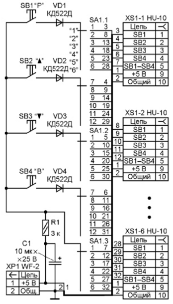
Encyclopedia of radio electronics and electrical engineering / Power Supplies The article describes a multi-channel phase regulator based on eight-bit microcontrollers AT89C4051-24PU. The device includes a switching unit and six phase regulators, each of which is capable of controlling two loads with a power of 1,15 kW each (limited by the capabilities of the applied mains filters). In addition, each of the dual regulators has a real time clock. The device is made on an accessible element base and can be repeated by medium-skilled radio amateurs. The block diagram of the 12-channel phase controller is shown in fig. 1. Here A1-A6 are two-channel phase power regulators identical in scheme, design and operation algorithm; S1 - switching unit, with the help of which power control is carried out, setting the current time and the time of operation of two alarms. A schematic diagram of one two-channel power controller is shown in fig. 2, and the switching unit - in fig. 3.
Sockets XS1-1 - XS1-6 of the switching unit are designed to connect XP4 plugs of regulators 1-6. Each regulator has two independent phase regulators and, in addition, the functions of an electronic clock are implemented. Details about the controller and its functions will be described below. Switch SA1 of the switching unit has six positions. If it is set to "1", then the SB1-SB4 buttons are connected to controller 1 and you can set the parameters for this controller. Accordingly, if it is set to "2", you can set the parameters for knob 2, etc. Consider in detail the operation of the regulator 1 (SA1 - in position "1"). The device has the following functions: - two independent channels of phase-pulse regulation; - indication of the current time in 24-hour format on a four-digit display in the hour-minute mode ("Hour 2" mode); - setting the current time and its adjustment; - work in the minute-second mode ("Clock 1" mode); - two alarm clocks, at the moment of operation of which the loads connected to the connectors ХP5 and ХP6 (TV set, radio receiver, electric heater, etc.) are turned on, and intermittent light and sound signaling with a repetition rate of 10 Hz for 1 s; - giving a short (duration 1 s) sound beep signal at the beginning of each hour and forced shutdown of the light and sound signaling by the button at the moment the alarm goes off. Accordingly, six operating modes are provided: "Clock 1", "Clock 2", "Regulator 1", "Regulator 2", "Alarm Clock 1" and "Alarm Clock 2". Two independent power controllers are assembled respectively on simulators VS1 and VS2. Power control is carried out by phase-pulse control of triacs. The output power control interval of each channel is set in relative units from 0 to 99. Of course, phase-controlled regulators create noise, but they are easy to implement and allow you to control the power of loads such as incandescent lamps, heaters, AC induction motors and etc. The controller interface includes buttons SB1-SB4 (Fig. 3), LED strips HL1, HL2 and a display of six digital seven-element indicators HG1-HG6 (see Fig. 2). The purpose of the buttons is as follows:
In any operating mode of the device, each button performs only one function (except for turning off sound and light signals when alarms are turned on). The bits of the interface indication have the following purpose (from right to left in Fig. 2):
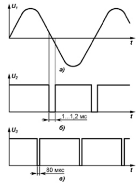
After turning on the power, the device enters the "Clock 1" mode. To set the current time, you need to enter the "Clock 1" mode by pressing the SB2 button (the number 1 should appear on the HG1 indicator), and then press the SB4 button once. This will select the digit of units of minutes (dot h at the indicator HG6 will start to glow). The required value of the discharge is set by the buttons SB2 and SB3. The next time you press SB4, the tens of minutes digit is selected (the h point turns on at the HG5 indicator), etc. After setting the value in the tens of hours digit (HG2 indicator), press the SB4 button again, thereby resolving time counting. To set the power value in channel 1, use the SB1 button to select the "Regulator 1" mode of operation (the number 1 should be lit on the HG2 indicator). Then use the SB4 button to select the category and use the SB2 ("More") and SB3 ("Less") buttons to set the required power value. When setting the time in the "Clock 2" mode, the countdown of the current time is prohibited, in all other modes it is allowed. After setting the time of alarm clocks 1 and 2 (the enumeration of the digits with the SB4 button is completed), the light strips HL1 and HL2 light up, respectively. The luminous strip indicates that the set alarm time is recorded in the memory of the microcontroller (if necessary, it can be reprogrammed). If the current time coincides with the set time in the "Alarm Clock 1" and "Alarm Clock 2" modes, intermittent sound (HA10) and light (HL1) alarms are switched on for 1 s with on and off intervals of 0,5 s. At the end of this time, the switched on light strip HL1 goes out. Let's consider the main functional units of regulator 1 (see Fig. 2). Its basis is the DD1 microcontroller, the operating frequency of which is set by an oscillator with an external ZQ1 quartz resonator at 10 MHz. A mains voltage sensor is assembled on the transistor optocouplers of assembly U1. It monitors the moments when the mains voltage passes through zero. The output voltage of the sensor from the resistor R8 is fed to pin 7 of the microcontroller. Power control channel 1 is assembled on a triac VS1 and an optocoupler U2 and is controlled by a signal from pin 8 DD1. The load is connected to the XP2 connector. The second channel is assembled on triac VS2 and optocoupler U3 and is controlled by a signal from pin 9 of the microcontroller. The load is connected to the XP3 connector. To reduce the level of interference generated by the regulators, they are included in the network through line filters Z1 and Z2. Dynamic indication is made on microcircuits DD2, DD3, transistors VT1-VT5 and digital seven-element indicators HG1-HG6. The DD2 register serves to increase the number of microcontroller port lines and controls internal actuators: sound and light alarms (respectively, a piezoelectric emitter HA1 and light strips HL1 and HL2), triac optocouplers U4, U5, as well as a discharge on the indicator HG1. Resistors R9-R15 limit the current through the elements of digital indicators. The signal from output 3 (pin 6) of register DD2 through resistor R26 periodically (with a period of 1 s) turns on and off the element g of the HG4 indicator in the "Clock 1" and "Clock 2" modes. The signal from output 4 (pin 9) of register DD2 through resistor R27 includes point h in one of the selected indicators HG2, HG3, HG5, HG6. The digital part of the device is galvanically isolated from the network. The microcontroller program controls the operation of the electronic clock and provides the implementation of pulse-phase control of triac power controllers. The main task of the "hourly" part of the program - the formation of accurate time intervals with a duration of 1 s - is solved using interrupts from the TF0 timer. In the TF0 timer interrupt routine cycle, every 80 µs, the microcontroller polls the status of pin 7. The counters on registers R4, R6 count the number of interrupts, and when it becomes equal to a certain value, the current time increases by a second. The current time is updated every hour. In this device, the clock lags behind by about 6 s per day, which is quite acceptable in everyday life. The TF0 timer interrupts also provide dynamic indication. Let's conditionally call the bytes that the microcontroller periodically (with a period of 3 ms) writes to its port P1 and the synchronous register DD2, respectively, as indication and status bytes. The lower tetrad of the indication byte is fed to the input of the decoder DD3 and determines the value of the bit, and the bits of the higher tetrad through the transistors VT2-VT5 control the indicators HG2, HG3, HG5, HG6 in dynamic indication. Transistor VT1 and, accordingly, the HG1 indicator are controlled by a signal from pin 12 of register DD2. In the "Regulator 1" and "Regulator 2" modes, the HG2 and HG3 indicators go out. To extinguish the indicator, it is necessary that the code F is present in the low tetrad of the indication byte. log level. 0 at pin 16 of the microcontroller opens transistor VT2 and turns on indicator HG2, a signal of the same level at pin 17 opens transistor VT3 and turns on indicator HG3, etc. The lower tetrad is a binary-coded decimal number and controls the elements of all indicators through the decoder DD3, except HG4. With the indicators HG2, HG3, HG5, HG6 on, the microcontroller polls the status of its INTO input (P3.2; pin 6 DD1). When any button SB1-SB4 is pressed, there is a low level at this input with the inclusion of the indicated indicators. Thus, each button of the switching unit is "tied" to its "own" bit in the upper tetrad of the indication byte. We will consider the algorithm of the program of the phase-pulse controller using the example of channel 1. The oscillograms explaining the operation of the controller are shown in fig. 4. In each half-cycle of the mains voltage (Fig. 4, a), the microcontroller, with a triggering pulse from output 8 with a duration of 80 μs (Fig. 4, c), turns on the triac VS1 through the optocoupler U2. The power value in the load connected to the XP2 connector depends on how long the triac is on during each half cycle of the mains voltage. In order for the power value in the load to increase with an increase in the value of the set power on the device indicator, and also to obtain a control discreteness equal to 1%, it is necessary that the triac turn-on pulse shift (from right to left in Fig. 4,b) with a step of 100 μs from the moment the mains voltage passes through zero with an increase in the value of the set power on the device indicator by one.
The triggering pulse is given with some delay relative to the moment when the mains voltage passes through "zero". The moment of the transition corresponds to the log. 0 at pin 7 of the microcontroller (Fig. 4b). The delay time is determined by the number on the indicator of the device in the "Regulator 1" mode, which can take a value from 0 to 99. The subroutine converts this two-digit binary-decimal number to one-byte binary. This number is loaded into the counter (register R7) which implements the time delay. As already mentioned, the microcontroller polls the network sensor output every 80 µs. At the moment the mains voltage passes through zero, the counter starts. When the button changes the number displayed on the indicator in the "Regulator 1" mode, the delay time for turning on the control pulse to turn on the triac VS1 changes. That is, the moment of turning on the triac in each half-cycle of the mains voltage and the effective voltage on the load connected to the XP2 connector change. The second channel of the device operates similarly, regulating the power in the load connected to the XP3 connector. The angle of regulation of the triac, depending on the outflow of the load, is not the same. In reality, in the device, the interval for regulating the power of a 100-watt incandescent lamp according to the indicator is from 18 to 97. In other words, 79 brightness levels can be set. This is necessary when the lamp is used as a heating element. For a faster change in brightness (for illumination, as practice shows, such a large number of levels is not necessary), you can change only the highest bit of the relative range of regulation of the specified power. Briefly about the program. In the data memory of the microcontroller from address 2BH to 48H, a display buffer is organized for dynamic indication. The lower tetrad of each byte in the display buffer is a binary-coded decimal number that specifies the bit value, and the upper tetrad specifies the bit number in the dynamic display. Thus, in each byte of the buffer, the value of the number and its place when displayed are determined. According to its functional purpose, depending on the operating mode of the device, the buffer address space is divided into six functional groups:
Each byte from the cycle function group in the TF0 timer interrupt routine is output to the P1 port of the DD1 microcontroller. The upper tetrad of the indication byte is a "running zero" code. Thus, writing in a cycle bytes from the functional group of the buffer alternately to the P1 port, we get a dynamic indication mode. After the indication byte is written to the P1 port, the polling of the buttons begins. By pressing the SB1 button, the unit in register R2 is shifted to the left and thus one of the above five operating modes is set. Register R0 is written to the first address of the functional groups. The R3 register is incremented every 0 ms in the interrupt routine. In the main program, the calculation and correction of the current time, setting the time for turning on alarms, comparing the current time with the alarm time, turning on light and sound signals, converting a two-digit binary-decimal number (the value of the set power level on the device indicator) in the "Regulator 1" and "Regulator 2" to a one-byte binary to implement the phase-pulse control algorithm. The developed program in assembler occupies about 3,7 kB of microcontroller program memory. Each of the regulators and the switching unit are mounted on separate prototyping boards 120x80 mm in size. When installing regulators, it is desirable to separate the digital part of the device from the network. All resistors are S2-33N with a dissipation power of 0,125 W, but any others with the same dissipation power and a tolerance of ± 5% of the nominal resistance will do. Capacitors C1, C4 - imported oxide, C2, C3 - ceramic K10-17. Between the power outputs (+5 V and a common wire) of the DD1 microcontroller and the DD2 register, it is useful to install blocking capacitors K10-17 with a capacity of 0,1 μF. In the display, it is advisable to highlight the digit indicating the current mode of operation of the device (indicator HG1), against the background of other digits. Therefore, for this discharge, a seven-element red glow indicator HDSP-F001 was selected (HDSP-F151 is suitable); indicators HG2-HG6 - green glow HDSP-F501 (any others with a common anode and acceptable brightness will do). In the HG4 indicator, only the g segment is used to form the "-" sign. The current through the indicator elements is determined by the load capacity of the DD3 decoder. For KR514ID2, the maximum allowable current for each output is 22 mA. Light strips HL1, HL2 - №-2300EW red glow. The current through each power control channel is limited by the maximum allowable current of 5 A through the mains filter FS-220 (Z1, Z2). At light loads, and also if the requirements for the level of interference are not very high, mains filters can be omitted. Loads are connected to the device through MPW-2 plugs (the counterpart is MHU-2 sockets). Instead, you can use terminal blocks TV-10-2. If the rated load power in the control channel exceeds 100 W, then the triac should be installed on an appropriate heat sink. The TIC236M triac, whose permissible current is 12 A, allows you to control a load with a power of up to 1,5 kW. A possible replacement is the domestic triac KU208G, however, it has a much worse sensitivity: for reliable operation, a current of at least 250 mA must flow through the control electrode of this triac, so the resistance of resistors R1 and R3 must be reduced to 100 ohms. For loads up to 2 kW, triacs with a permissible current up to 16 A can be used, for example ^C246N. It is advisable to measure the actual values of the control and holding current of the applied triacs in order to assess the suitability of the triac for working with a specific, especially low-power load. The triac optocouplers S202SE2 from SHARP (U4, U5) used in the device can switch current up to 8 A. They are switched on near the zero crossing of the mains voltage. It is possible to use optocouplers S202S02, and if the switched current in the load does not exceed 2 A, then S202TO1. The current consumption from the 5 V power supply in the power regulators does not exceed 80 mA. Capacitor C1 of the switching unit is imported oxide. Salt switch SA1 - PG2-12-6P8N (six positions and eight directions). Pushbutton switches SB1-SB4 - PKN125 or similar. The device does not provide for any settings and adjustments, and if the installation is done correctly and all the parts are in good order, then it starts working immediately after the supply voltage is turned on. When checking power control channels, it is better to turn on the first switch at a low load, for example, with an incandescent lamp with a power of 20 ... 30 W. It is advisable to first check the power control channel 1, and then 2. To do this, enter the "Regulator 1" mode and, by changing the power level using the indicator from the keyboard, control the change in the brightness of the lamp. If the lamp does not turn on at all, then you need to check the signal from the network sensor (pin 7 of the DD1 microcontroller) - the presence of pulses with a log level. 0 with a duration of 1...1,2 ms and a period of 10 ms (Fig. 4b). Author: S. Shishkin
Machine for thinning flowers in gardens
02.05.2024 Advanced Infrared Microscope
02.05.2024 Air trap for insects
01.05.2024
▪ Everyone has their own reality ▪ Aspirin is the culprit of death ▪ SanDisk iNAND 7132 Embedded SSD
▪ section of the site Amateur Radio Technologies. Selection of articles ▪ Gulliver article. Popular expression ▪ article Why is electricity called electricity? Detailed answer ▪ article Head of Innovation Department. Job description ▪ article Touch relay. Encyclopedia of radio electronics and electrical engineering
Home page | Library | Articles | Website map | Site Reviews
www.diagram.com.ua |


 Leave your comment on this article: