|
|


 Arabic
 Bengali
 Chinese
 English
 French
 German
 Hebrew
 Hindi
Hindi Italian
 Japanese
 Korean
 Malay
Malay Polish
 Portuguese
 Spanish
 Turkish
 Ukrainian
 Vietnamese
|
ENCYCLOPEDIA OF RADIO ELECTRONICS AND ELECTRICAL ENGINEERING Stabilized power supply UMZCH. Encyclopedia of radio electronics and electrical engineering
Encyclopedia of radio electronics and electrical engineering / Power Supplies Modern UMZCH, having an impressive peak output power, sometimes reaching up to 200 W, impose rather stringent requirements on their power source. For them, as a rule, a bipolar voltage of 2 X (30 ... 40) V is required with a peak current of up to 10 A in each arm. Usually, high-capacity smoothing capacitors are used in the rectifier, reaching up to 20000 microfarads or more. But even with them, the rectified voltage drawdown at peak load current reaches 2 ... 3 V, which requires a high coefficient of suppression of supply voltage ripples from the UMZCH. The author proposes to equip the UMZCH power supply with a stabilizer that provides the desired quality of the supply voltage. Recently, in amateur UMZCH designs, a rectifier and a block of large-capacity capacitors are increasingly located on the amplifier board, thereby reducing the length of the connecting wires and the voltage drop across them. Sometimes it is required from the power supply that, when turned on, the voltage at its outputs increases smoothly (the so-called "soft start"). In the event of various emergency situations, for example, a short circuit in the UMZCH load, a malfunction of its output transistors and other overloads, the UMZCH power supply should be automatically turned off. The proposed supply voltage stabilizer can solve all these problems. Main Specifications
The design was based on the device from the article "UMZCH Supply Voltage Stabilizer" by V. Oreshkin ("Radio", 1987, No. 8, p. 31), the diagram of which is shown in fig. 1. Despite the simplicity and high technical data (stabilization coefficient of more than 1000, automatic shutdown when the output is closed, the ability to attach power transistors directly to the heat sink without gaskets), this stabilizer also has some disadvantages. It starts up unstable at a high load current, and the current when the output is closed is not normalized and depends on the transfer coefficients of the transistors used, which sometimes leads to their failure.
Recently, new electronic components have appeared, powerful field-effect transistors have become available, which prompted the author to experiment with a computer model of the device proposed by V. Oreshkin, which was created in the LTspice IV simulator, and improve it. The power supply circuit that was born as a result of such experiments is shown in Fig. 2.
First of all, the stabilizer trigger circuit was changed, and the bipolar transistors were replaced with field ones. From the scheme presented in fig. 1, it can be seen that the transistor VT2 is shunted by a resistor R3 with a resistance of 470 ohms, through which the initial charging current of the capacitor C2 flows. If the load is small, the output voltage starts to increase until the regulator enters stabilization mode. At load current less than I=UO/ R3 = 19/470 = 40 mA, when the transistor VT2 is almost closed, all ripples of the rectified voltage through the resistor R3 pass into the negative shoulder. With a low load resistance, the current through this resistor may not be enough to start the stabilizer normally, it may not start at all. In the new version, the start circuit consists of a zener diode VD11 and a resistor R22 in one arm and VD12 with R23 in the second (for symmetry). In the process of switching on, upon reaching the voltage value on the smoothing capacitors C7-C10, equal to the stabilization voltage of the zener diodes VD11 and VD12, the transistors VT 11.1 and VT11.2 begin to open. Following them, power transistors VT9 and VT10 open. The voltage at the output of the stabilizer increases, and the voltage between the source and drain of transistors VT9 and VT10 decreases. When the voltage on the zener diodes VD11 and VD12 drops below their stabilization voltage, the current through these zener diodes will stop. Further, they do not affect the operation of the stabilizer. This way of starting is reliable even with a load current of 9 A. The minimum load current is almost zero. The output voltage of the positive arm of the stabilizer is equal to the sum of the stabilization voltages of the zener diodes VD13, VD15 and the cutoff voltage of the transistor VT11.1, and the negative arm is equal to the sum of the zener diodes VD14, VD16 and the transistor VT11.2, respectively. For a smooth start of the stabilizer, it turned out to be enough to shunt the VD13-VD16 zener diodes with capacitors C23-C26. The rate of change of the output voltage before stabilization is equal to the rate of voltage rise across these capacitors. With the ratings of the elements indicated in the diagram, the time for the stabilizer to enter the mode is about 360 ms. Oscillograms of the process of its launch, obtained on a computer model, are shown in fig. 3.
To reduce the power dissipated on transistors VT9 and VT10, the sources of transistors VT 11.1 and VT 11.2 are not connected to a common wire, but to the connection points of zener diodes and resistors (VD15, R29 and VD16, R30, respectively). Therefore, the potentials of the sources of transistors VT11.1 and VT11.2 are equal to the stabilization voltage of the corresponding zener diodes (6,2 V in absolute value). This allows you to change the control voltage at the gates of transistors VT9 and VT10 not to 0 V, as in the prototype, but to plus or minus 6 V. At the same time, the voltage between the source and drain of these transistors at the peaks of ripples can drop to 3 V and below without leaving stabilization mode. The foregoing is illustrated by the oscillograms obtained by computer simulation in Figs. 4. Green - voltage at the source of the transistor VT10, blue - voltage at its gate, red - voltage at the source of the transistor VT11.2 (6,2 V), blue - load current of the negative arm. It can be seen that the voltage at the gate of the VT10 transistor lies approximately in the middle between the voltage at its source and at the source of the VT11.2 transistor, and sometimes drops below 3 V.
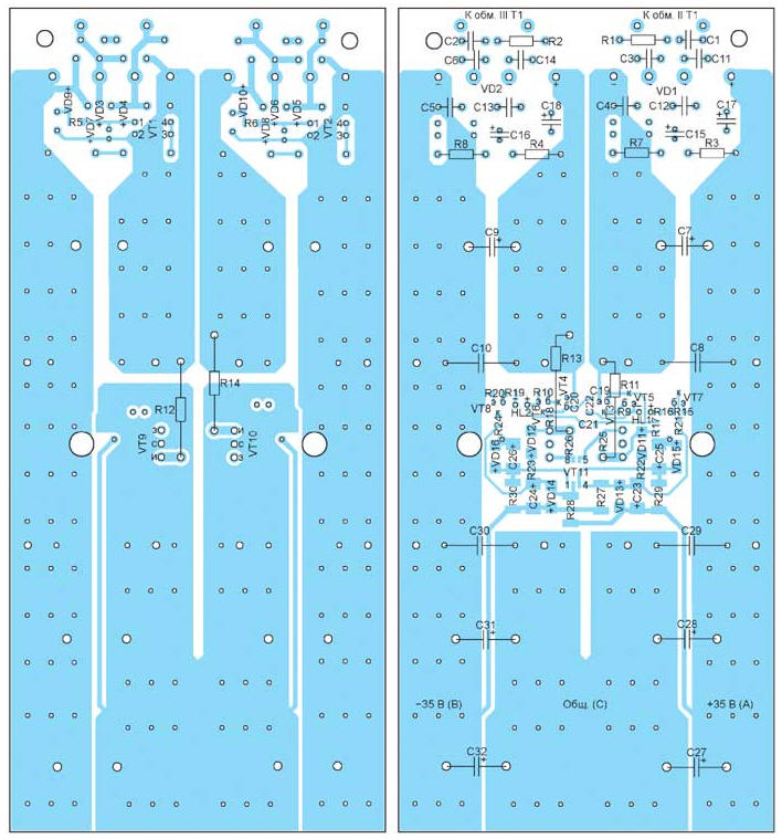
A current trigger protection has been added to the stabilizer, which is triggered when the load current of any branch of the stabilizer exceeds 11 A. It is built on transistors VT3, VT5, VT7 in the positive shoulder and VT4, VT6, VT8 in the negative. Current sensors are resistors R11-R14, connected in pairs in parallel. The protection is triggered when the voltage drop across any of the pairs of resistors is more than 0,5...0,6 V, which corresponds to the current flowing through them 11...12 A. Upon reaching this threshold, the transistors of the trigger cells VT3VT5 or VT4VT6 and, accordingly, the transistors VT7 and VT8 open like an avalanche. The latter, having opened, shunt the zener diodes VD13 and VD14, thereby sharply lowering the output voltage. Resistors R21 and R24 limit the collector current of the transistors when discharging capacitors connected in parallel with the zener diodes. LEDs HL1 and HL2 in the base circuits of transistors VT7 and VT8 signal the protection operation. The current through them does not exceed 6 mA. Capacitors C19 and C20, together with resistors R17 and R18, form low-pass filters that increase the noise immunity of the protection system. It is undesirable to increase the ratings of these capacitors above 4700 pF, since this will increase the protection response time and peak currents through the VT9 and VT10 transistors. In order for the protection to work simultaneously in both arms of the stabilizer, a connection is provided between the trigger cells through capacitors C21 and C22. After the protection is triggered, transistors VT9 and VT10 remain closed until the device is disconnected from the mains. The transistors of the trigger cells will close, and the HL1 and HL2 LEDs will go out only after the smoothing capacitors C7-C10 are discharged. One problem remains - to ensure that the smoothing capacitors discharge quickly after switching off. It is solved by nodes on transistors VT1 and VT2, which are the same in both channels. Therefore, we will consider only the node installed in the positive channel. When the device is connected to the network, the capacitor C17 is charged through the diode VD9 to a voltage approximately equal to the amplitude of the voltage coming from the winding II of the transformer T1. Capacitor C15 is charged through resistor R5 and discharged through diodes VD3, VD4 and diode bridge VD1. The gate potential of the transistor VT1 becomes equal to the potential of its source or even slightly lower, so the transistor is closed. The closed state of the transistor VT1 is maintained throughout the entire time while the supply voltage is applied. After it is turned off, the diodes VD3 and VD4 close. The gate-source voltage of the transistor, thanks to the resistor R5, increases to the stabilization voltage of the zener diode VD7. Having opened, the transistor VT1 connects the resistors R3 and R7 in parallel with the capacitors C7 and C8, accelerating their discharge. The discharge duration is reduced to 10...20 s at a peak value of the discharge current of 780 mA, which is quite acceptable for the transistors used. On fig. 5 shows a drawing of printed conductors of a board with dimensions of 175x80 mm, on which the described power supply was assembled. It is made of fiberglass foiled on both sides with a thickness of 1,5 mm. Foil thickness - not less than 50...70 microns, and better - 110 microns. The placement of parts on the board is shown in fig. 6, its appearance - in Fig. 7. Transistors VT9 and VT10 are mounted on the conditionally lower side of the board and fixed on the heat sink. Holes are provided on the board to access the screws that secure the transistors.
Basically, surface-mount resistors of size 0805 are used, and resistors R27-R30 are of size 2512 (1 W). Resistors R1-R4, R7, R8 - MLT or similar imported ones. Resistors-current sensors R11-R14 - KNP-100. They are installed on both sides of the board. Instead of each pair of these resistors, one half the resistance and a power of 1 ... 2 W can be used. Capacitors C1-C6, C8, C10-C14, C29, C30 - metal-film K73-17 for a voltage of at least 63 V or their imported analogues. Capacitors C19-C22 - ceramic for surface mounting, size 0805 or 1206. Oxide capacitors C23-C26 - tantalum sizes D or E, C7 and C9 - aluminum series LS from Jamicon, C27, C28, C31, C32 - aluminum series RD from SAMWHA, the rest - K50-35 or similar imported ones. Zener diodes DL4751A and DL4735A can be replaced by others with a stabilization voltage of 30 V ± 5% and 6,2 V ± 5%, respectively, in the MELF package. In the absence of GBJ2502 diode bridges, others can be installed instead of them for a current of 25 A with a permissible reverse voltage of at least 100 V, or each bridge can be assembled from four single Schottky barrier diodes with suitable parameters. Replacing diodes RS1B - diodes of the same series or any low-power ones with a reverse voltage of at least 60 V. Field-effect transistors IRFD024 can be replaced by other N-channel insulated gate transistors with a permissible drain-source voltage of 50 ... 60 V, for example, IRFZ24, IRFZ34, IRFZ44, but the PCB will need to be adjusted. Instead of BSS63 and BSS64 transistors in overload protection units, it is permissible to use any low-power general-purpose bipolar transistors of the appropriate structure in the SOT23 package with a maximum collector-emitter voltage of at least 50 V. As a replacement for the IRF1405 and IRF4905 transistors, powerful field-effect transistors with an insulated gate, the highest speed and a large slope of the characteristic, should be selected. It is also necessary that they have a minimum threshold source-gate voltage. A microassembly of two field-effect transistors with channels of different types of conductivity IRF7343 can be replaced with FDS4897C or FDS4559. If you reduce the input and output voltage of the stabilizer, respectively, to 30 V and 27 V, then you can use the IRF7319 microassembly. The transistors of these microassemblies have a small (about 1 V) and almost identical gate-source threshold voltage in absolute value. You can, of course, use separate low-power field-effect transistors with a maximum drain-source voltage of at least 45 V, but in this case, the difference in the output voltage of the stabilizer arms can become larger. A properly assembled unit practically does not need to be adjusted, but nevertheless it is desirable to make the first switch-on with an incandescent lamp with a power of 40 ... 60 W, connected in series with the primary winding of the transformer T1. At the moment of switching on, it should light up, and then go out. After that, you should measure the output voltage, it should be within 35 ± 0,5 V. Briefly closing the output of one of the stabilizer arms with a powerful 3 Ohm resistor, make sure that the protection is triggered. After restoring the operation of the stabilizer, check with an oscilloscope that there are no visible ripples in the output voltage with the mains frequency. Below are oscillograms of real ripples of the output voltage of a stabilizer operating at UMZCH with a load of 4,7 ohms. On them, the yellow curve is the voltage at the output of the UMZCH, the blue one is the variable component of the voltage at the output of the stabilizer (between points A and C or B and C). Oscillograms were taken under the following conditions: rice. 8 - there is no signal at the UMZCH input, the quiescent current of the amplifier is 0,25 A; rice. 9 - UMZCH output voltage amplitude - 25 V, frequency - 10 kHz, ripple amplitude - less than 10 mV; rice. 10 - amplitude of pulses at the output of UMZCH - 20 V, frequency - 30 Hz.
It should be noted that the transformer T1 must be of sufficient power to provide a maximum load current of 10 A. The voltage across the smoothing capacitors of the rectifiers at the peak of the load current should not fall below 38 V. Considering the crest factor of the music signal, usually close to three, the power of the transformer for each channel, the UMZCH should be about 200 W or more. The author used a 180 W transformer on a toroidal magnetic circuit. Author: M. Muravtsev
Machine for thinning flowers in gardens
02.05.2024 Advanced Infrared Microscope
02.05.2024 Air trap for insects
01.05.2024
▪ Quantum teleportation using conventional equipment ▪ Low temperature lithium-ion battery ▪ Trillion frames per second camera
▪ section of the site Electrician's Handbook. Article selection ▪ article Forensic medicine. Crib ▪ article How and why did Ariadne help Theseus defeat the Minotaur? Detailed answer ▪ article How to dry shoes. Travel Tips ▪ article Phenomenal memory. Focus secret
Comments on the article: R'RёS,R ° F "RёR№ What needs to be changed to get 45 volts at the output? Andrei Where can I order printed circuit boards for the power supply author M. Muravtseva Tashkent, Uzbekistan
Home page | Library | Articles | Website map | Site Reviews
www.diagram.com.ua |


 Leave your comment on this article: