|
|


 Arabic
 Bengali
 Chinese
 English
 French
 German
 Hebrew
 Hindi
Hindi Italian
 Japanese
 Korean
 Malay
Malay Polish
 Portuguese
 Spanish
 Turkish
 Ukrainian
 Vietnamese
|
ENCYCLOPEDIA OF RADIO ELECTRONICS AND ELECTRICAL ENGINEERING Inverter source of welding current. Experience in repair and calculation of electromagnetic elements. Encyclopedia of radio electronics and electrical engineering
Encyclopedia of radio electronics and electrical engineering / welding equipment Inverter welding current sources (IIST), sometimes not quite correctly called high-frequency ones, have clear advantages over classical transformer ones (smaller mass and volume, excellent load characteristics), but they are not widely used in our country. Most likely, because of the high, inaccessible to most potential consumers, the cost. Many radio amateurs try to make their own IIST. However, significant difficulties arise along this path, primarily due to the lack of experience in the development of energy-intensive devices, in which the values of current and voltage go far beyond the usual limits. The author shares his experience in the repair of industrially manufactured IIST, which required the selection of failed power elements and rather significant changes in the circuit. The method of calculation of the main electromagnetic elements of IIST is given. At one fine moment, a faulty Castolin Eutectic RytmArc welding machine, released in 1988, fell into my hands. The former owner, no longer believing that the device could be repaired, gave it away for spare parts. When examining the device, it turned out that this typical representative of the family of low-power single-phase IISTs oriented to domestic use is made according to the scheme of a single-cycle forward half-bridge inverter typical for devices of this class and is intended for manual electric welding with a direct current of 5 ... 140 A with a relative welding duration of up to 100% welding/pause cycle. In the original version, the inverter was built on powerful high-voltage bipolar compound transistors ESM2953, which failed. Several lower power transistors also turned out to be faulty, and some parts were simply missing. In such a situation, the most justified decision seemed to be to buy new transistors and replace the burnt ones with them. However, the trading company that found the required transistors offered them at a price of $ 65 per piece, subject to the purchase of a whole package - 50 pieces. Naturally, this option did not work, and I had to look for an alternative. The choice fell on IRG1PC4U Insulated Gate Bipolar Transistors (IGBTs [50]), which were freely available at retail for $14 each. Unlike the ESM2953, the collector of the IRG4PC50U transistor is electrically connected to its heatsink base. Therefore, it was decided, by installing each IGBT on an aluminum plate with dimensions of 30x25x4 mm, to press the latter to the main heat sink through mica spacers 0,5 mm thick. Since mica of the required thickness was not available, the gaskets were assembled from several layers of thinner, "glued" heat-conducting paste. To start the IIST, it was necessary to develop and manufacture a new driver for controlling the IGBT and the lost timer for the charging current limiter of the filter capacitor of the mains rectifier. The control unit board, fortunately, did not require repair. The restored device has been functioning flawlessly for more than four years. The scheme of IIST after repair is shown in fig. 1, and its appearance with the cover removed is shown in Fig. 2, where the main elements are marked. Due to the lack of factory documentation, the item designations of the elements with the "branded" ones do not match.
The technical solutions used in this IIST are typical for devices of this class. For those who are going to repair or even construct such devices on their own, it is useful to familiarize themselves with its device in more detail.
When the switch SA1 is closed, an alternating voltage of 220V, 50Hz is supplied to the primary winding of the transformer T1, which supplies all the electronic components of the IIST (except for the inverter itself), and through the resistor R1, which limits the initial current surge, to the rectifier of two diode bridges VD1 and VD2 connected in parallel. The ripple of the rectified voltage is smoothed out by the oxide capacitor C2. After approximately 1 s required to fully charge this capacitor, a timer is triggered (its circuit is shown in Fig. 3) and the closed contacts of relay K1.1 shunt resistor R1, excluding the latter from the circuit of the current consumed from the network and thus eliminating the useless loss of energy.
In fact, two identical relays are installed in the IIST as K1, the windings and contacts of which are connected in parallel. Another relay K2, according to signals from the control unit board, turns the M1 fan on and off. The temperature-current converter VK1, mounted on a heat sink of powerful transistors, serves as a temperature sensor. The inverter on IGBT VT1 and VT2 converts the rectified mains voltage into a pulse frequency of approximately 30 kHz. Transformer ТЗ provides galvanic isolation between the welding circuit and the network. Its transformation ratio is chosen such that the amplitude of the pulses on the secondary winding is twice the specified open circuit voltage of the IIST. Details on the principle of operation of a single-cycle half-bridge inverter can be found, for example, in [2, 3]. The current transformer T2 is connected in series to the primary winding circuit of the transformer TK and is designed to control the current flowing here. In high-frequency switching inverters, the magnetizing and leakage inductances of the transformers, together with the parasitic inductance of the installation, accumulate significant reactive energy. Turning it into heat would lead to a significant decrease in the efficiency of the device. Therefore, using special circuit solutions, they try to transfer the accumulated energy to the load or recuperate - return to the power source. At the moments of change in the state of power switches, each inductance, including parasitic, becomes a source of voltage pulses of self-induction, often dangerous for the elements of the magnitude converter. Damping RC circuits with and without diodes are designed to reduce the amplitude of these pulses. To reduce the leakage inductance harmful to the operation of the IIST, it is desirable to use transformers with toroidal magnetic circuits, and a well-thought-out layout of the device reduces the installation inductance. The voltage of the secondary winding of the transformer TZ rectifies a half-wave rectifier on diodes located in four diode assemblies VD7-VD10 (two diodes each). Inductor L1, connected in series to the welding circuit, smoothes the rectified current. The control unit generates opening pulses for the IGBT inverter, adjusting their duty cycle in such a way that the external load characteristic of the IIST meets the requirements for high-quality electric welding. The controller inputs receive feedback signals for voltage (from the rectifier output) and current (from the secondary winding of the current transformer T2). The variable resistor R2 regulates the welding current. On fig. 4 shows a driver circuit that amplifies the pulses generated by the control unit to the amplitude required to control the IGBT VT1 and VT2. It was developed to replace the driver that controlled the bipolar transistors installed in the IIST before the repair.
Transformer T1 isolates the input circuits of two identical driver channels from the control unit and from each other. In this case, the transformer as an insulating element has an undeniable advantage over the optocoupler, since, with the right choice of parameters, it automatically limits the duration of the pulses arriving at the IGBT gates to a value at which the magnetic circuit of the power transformer TK is not yet saturated (see Fig. 1). The secondary windings II and III of the isolation transformer are connected in such a way that the channels work in phase, which is required for the correct operation of a single-ended inverter. Consider the operation of one of the channels - the upper one according to the scheme. Pulses from the winding II of the transformer T1 through the resistor R1 are fed to the input of the shaper, assembled on the DD1 chip. The power amplifier on transistors VT1 and VT2 provides fast charging and discharging of a rather significant capacitance characteristic of IGBTs between the gate and the emitter. Resistor R9 prevents oscillation in the circuit formed by the inductance of the connecting wire and the input capacitance of the IGBT. The rectifier and supply voltage stabilizer are assembled on a VD1 diode bridge and a DA1 chip. The alternating voltage to the rectifier comes from a separate isolated secondary winding of the transformer T1 (see Fig. 1). When manufacturing a driver, special attention should be paid to the quality of the isolation between its channels. It must withstand a voltage exceeding twice the amplitude of the mains. When embarking on the independent development of IIST, one has to face many issues that do not even arise during repairs - all of them have already been resolved in one way or another by the developers and the manufacturer. The greatest difficulties are associated with the choice of semiconductor devices that switch a large current at a relatively high voltage. The correct choice of the inverter circuit, the calculation and design of its electromagnetic elements is very important. In the absence of development experience, it is reasonable to strive to repeat "run-in" solutions. The problem is complicated by the fact that there is practically no literature in which one can find ready-made proven methods for designing IISTs. In [3], for example, the presentation is so concise that the calculations available there are practically impossible to extend to the specific problems of developing a welding source. In the material presented below, the conclusions of the calculated ratios are presented in some detail. According to the author, this will allow radio amateurs to better understand the processes occurring in the electromagnetic components of the IIST and, if necessary, correct the stated methodology. Under conditions of such a sharply variable load as a welding arc, a single-cycle forward half-bridge inverter compares favorably with others. It does not require balancing, is not subject to such a disease as through currents, a relatively simple control unit is enough for it. Unlike a flyback inverter, the shape of the current in the elements of which is triangular, in a forward inverter it is rectangular. Therefore, at the same load current, the amplitude of current pulses in a forward inverter is almost two times less. POWER TRANSFORMER CALCULATION A common feature of all single-cycle inverters is operation with one-sided magnetization of the magnetic circuits of power transformers. When the magnetic field strength changes from zero to maximum and vice versa, the magnetic induction B changes in the range from maximum Bm to residual Br. On fig. 5 shows a simplified diagram of a single-cycle forward half-bridge inverter.
When transistors VT1 and VT2 are open, the energy of the primary voltage source is transferred through the transformer T1 to the load. The magnetic circuit of the transformer is magnetized in the forward direction (section 1-2 in Fig. 6). After the transistors are closed, the current in the load is supported by the energy stored by the inductor L1. In this case, the circuit is closed through the VD4 diode. Under the action of the EMF of the self-induction of the winding I, the diodes VD1 and VD2 are open, the demagnetization current of the magnetic circuit flows through them (section 2-1 in Fig. 6).
The induction in the magnetic circuit changes only by ΔВ1 = Bm-Br1, which is much less than the value of 2Vm possible in a push-pull inverter. However, at zero field strength, the induction will be equal to Br1 only in a magnetic circuit that does not have a non-magnetic gap. The latter will reduce the residual induction to the value of Br2. It follows from [4] that the new value of the residual induction corresponds to the point of intersection of the original magnetization curve with a straight line drawn from the origin at an angle Θ:
where μ0 is the absolute magnetic permeability (the ratio of magnetic induction to the magnetic field strength in vacuum, a physical constant equal to 4π-10-7 H/m); lc is the average length of the magnetic field line; δ is the length of the non-magnetic gap. As a result of introducing a gap of length δ, the range of induction in the magnetic circuit will increase to ΔВ2=Вm-Br2. Our industry does not produce magnetic circuits specifically for IIST. To make an inverter power transformer, you can use magnetic circuits designed for television line transformers. For example, the PK40x18 magnetic circuit from the TVS-90LTs2 transformer (used in ULPCT TVs) has a cross section of 2,2 cm2, a window area of 14,4 cm2, and an average length of the magnetic field line of 200 mm. It is made of manganese-zinc ferrite M3000NMS1, designed to operate in strong magnetic fields, as indicated by the index C in the designation [5], and has the following parameters of the hysteresis loop: Bs=0,45 T (at H=800 A/m) , W=0,33 T (at H=100 A/m and T=60°C), Bg=0,1 T, Hc=12A/m. Under conditions of one-sided magnetization, the range of induction in this magnetic circuit, assembled without a gap, will not exceed 0,23 T. Let's set ourselves the goal of using a non-magnetic gap to reduce the residual induction to 0,03 T, which will increase the range of induction to 0,3 T. Assuming that the dependence B=f(H) when the field strength changes from -Нс to zero is practically linear, we find the change in induction in the section from 0 to Br2. To do this, let's draw a horizontal line at the level of Br2 until it intersects with the magnetization curve and find the negative field strength in the magnetic circuit -H1=8,4 A/m, corresponding to this induction. In our case
From (1) we find the length of the non-magnetic gap:
Field strength in the gap at maximum induction Vm=0ZTl
Ampere-turns of magnetization of the magnetic circuit
In idle mode, the input voltage of the inverter (U1, see Fig. 5) is equal to the peak value of the mains (310 V). Taking into account the voltage drop across the key transistors and the active resistance of the winding, it can be assumed that a voltage of 300 V is applied to the primary winding of the transformer. The open-circuit output voltage of the source in idle mode should be 50 V. The calculation will be made for the case when the pulse duration is equal to half the period, which corresponds to the maximum range of induction in the magnetic circuit. Under these conditions, a secondary voltage pulse amplitude of 100 V is required (twice the required value of the open circuit voltage). Therefore, the transformation ratio of the power transformer must be equal to
It should be noted that the influence of the leakage inductance of the transformer windings is not taken into account here. Its presence leads to a higher than the calculated value of the open circuit voltage. The effective value of the current of the secondary winding, which has the form of rectangular pulses, is related to the average, equal to the welding current iCB, by the ratio
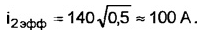
where λ is the ratio of the pulse duration to the period of their repetition (duty cycle). With iCB = 140 A and λ = 0,5
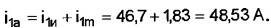
Effective value of primary winding current (excluding magnetizing current)
The amplitude of the load current pulse in the primary winding
At a frequency of 30 kHz, the energy losses in the ferrite core can be neglected. The losses in the winding wires increase with increasing frequency due to the displacement of the current to the surface of the conductor, which leads to a decrease in its effective cross section. This phenomenon is called the surface or skin effect. It manifests itself the stronger, the higher the frequency and the larger the diameter of the drive. To reduce losses, a stranded wire of thin insulated conductors is used - litz wire. To operate at a frequency of 30 kHz, the diameter of each of them should not exceed 0,7 mm [3]. The EMF of one turn is calculated by the formula
where dФ/dt is the rate of change of the magnetic flux coupled to the coil; ΔB - range of induction in the magnetic circuit, T; Sc - cross section of the magnetic circuit, cm2; tM - pulse duration, s; f - pulse repetition rate, Hz. The number of turns that fit in the window of the magnetic circuit can be found by the formula
where S0 - window area, cm2; - the coefficient of its filling with a wire (we will take equal to 0,25); ieff - effective current value; J is the current density in the winding wire, A/mm2. To determine the parameters of the magnetic circuit, we introduce a conditional value equal to the product of the voltage amplitude on the winding and the effective value of the current flowing through it. Since it has the dimension of power, let's call it the conditional power
In our case
Let us take the current density in the transformer windings J = 4 A/mm2, the range of induction in the magnetic circuit ΔB = 0,3 T, and from (2) we find
The W-shaped magnetic circuit required for the calculated transformer can be assembled from four PK40x18, as shown in Fig. 7.
We get a magnetic core with Sc=8,8 cm2, So-14,4cm2, ScS0=126,7cm4. Let's find for him the EMF of one turn
Number of turns of the primary winding
We choose it equal to 21 - the nearest larger integer, a multiple of the transformation coefficient (Ktr = 3). Number of turns of the secondary winding
The shape of the current in the primary winding of a power transformer is shown in fig. eight.
The amplitude of its magnetizing component is
Maximum current value of transistor switches and primary winding
To accurately calculate the effective value of the current of the primary winding, you will have to turn to the integral calculus:
An accurate calculation gives 33,67 A, which differs from the previously calculated value (33,3 A) without taking into account the magnetization current by only 1%. Cross section of winding wires:
When winding with a litz wire, recruited from insulated wires with a diameter of 0,55 mm, a bundle of 36 wires is required for the primary winding, and 105 wires for the secondary. Winding a transformer with a litz wire requires some experience. First of all, you need to prepare a litz wire. To do this, at a distance slightly greater than its required length, two hooks are fixed, the role of which can be successfully performed by door handles. Between the hooks pull the required number of wires. With the help of a hand drill or a brace, the bundle is twisted, periodically shaking slightly so that the wires in it are distributed evenly. The finished tourniquet is wrapped along its entire length with a slight overlap with a strip of thin cotton fabric 8 ... 10 mm wide. The windings are wound on a wooden mandrel, repeating the shape of the core of the magnetic circuit with a small margin, so that the finished coil freely "sits" in its intended place. The mandrel is provided with removable cheeks, the distance between which is 2...3 mm less than the height of the magnetic circuit window. Before winding, pieces of a keeper tape are laid on the mandrel, with which the finished coil is subsequently pulled together. The windings are arranged in the usual order: primary, on it - secondary. Insulation is required between them - a layer of electric cardboard 0,5 mm thick. The coil is given a shape corresponding to the configuration of the magnetic circuit window, then impregnated with varnish. The winding terminals must be provided with brass lugs. When embedding a litz wire in them, pay special attention so that the ends of all the wires that make up it are stripped of insulation, tinned and securely soldered to the tips. Calculation of the welding current filter choke Choke L1 (see fig. 1 and 5) smoothes the welding current. During the action of the secondary voltage pulse, the current in it linearly increases. During the pause between pulses - linearly decreases. The amplitude of the current ripple in the first approximation does not depend on its average value - the welding current. At the minimum value of the latter, the current in the inductor and in the welding circuit drops to zero by the end of the period. This is exactly the situation shown in Fig. 9.
A further decrease in the average value of the current leads to a violation of the continuity of its flow - for some part of the period, the current is zero, which leads to instability and extinction of the arc. The ratio between the amplitude and average values of the current of a triangular shape can be found from the condition of equality of the areas of the triangle formed by the current curve and the time axis, and a rectangle with a height icp built on the same axis (shaded in the figure). The length of the bases of both figures is equal to the period of oscillation. Thus,
At the minimum welding current isv. min=5 A voltage drop across the arc Ud. min can be considered equal to 18 V [6]. Given that
find the minimum required inductance of the inductor
The choke winding must withstand the maximum welding current icv. Max. Assuming, as for the transformer, the window filling factor ko = 0,25 and the current density J = 4 A / mm2, we determine the maximum possible number of turns of the inductor winding
Knowing the cross section of the magnetic circuit Sc and the coefficient of its filling with steel kс, it is possible for a given induction B in the magnetic circuit to determine the flux linkage of the inductor winding
Substituting (4) here, we get
Given that
find the inductance of the inductor
and the product SCSo for its magnetic circuit
To avoid saturation, the magnetic circuit must have a non-magnetic gap, due to which the induction changes from almost zero to W. Assuming that the inductor magnetic circuit is ideal and all ampere-turns of the winding are applied to the non-magnetic gap, we determine the length of the last b, mm:
whence
From (5), (6) and (9) we obtain a formula for calculating the actual inductance of the inductor:
Since at a welding current greater than the minimum, the amplitude of the magnetic flux ripples in the inductor magnetic circuit is insignificant compared to its average value, the magnetic circuit is usually made of electrical steel, for which the maximum induction is Vm-1 T. Assuming the filling factor of the section with steel kс=0,9, from (7) we find
Let us choose for the inductor a standard tape magnetic core ШЛ25х32 with Sckc=6,56 cm2, So=16 cm2 and SCSo=125 cm4. Using formula (4), we determine the number of turns
Using formula (8), we calculate the length of the non-magnetic gap
Such a gap will be provided by two non-magnetic spacers 1 mm thick, installed between the ends of the halves of the magnetic circuit. Choke winding wire cross section
The wire can be solid or assembled from 147 wires with a diameter of 0,55 mm. Using formula (10), we check the resulting inductance of the inductor
It exceeds the minimum value calculated above. Current transformer calculation On fig. 10 shows a diagram of the node for generating a current feedback signal.
The primary winding of the current transformer T2 is a brass stud with a diameter of 8 ... 10 mm, connecting the output of the inverter with the power transformer T1 (Fig. 2). "Penetrating" the control board, the pin passes through the window of the magnetic circuit of the T2 transformer installed there. The secondary winding wound on the magnetic circuit consists of ten turns, so that the transformation ratio KT0,1 = XNUMX. During the forward run of the inverter, the current of the secondary winding of the transformer T2 flows through the diode VD2 and a shunt of six parallel-connected resistors R3-R8 of 2,2 ohms each. From the shunt, the current feedback signal enters the control unit, where it is used to form a steeply falling load characteristic of the IIST and to protect the device from current overloads. During the reverse stroke, the polarity of the voltage on the secondary winding of the transformer T2 is closing for the diode VD2 and opening for VD1. The latter is open, and the demagnetization current of the transformer magnetic circuit flows through resistors R1, R2 connected in parallel. Since their total resistance is greater than that of resistors R3-R8, the magnetic circuit is guaranteed to demagnetize during the reverse stroke. The effective value of the current of the secondary winding of the transformer T2
Assuming the current density in the secondary winding of the current transformer J = 5 A / mm2, we find the diameter of its wire by the formula
At a frequency of 30 kHz, it is not recommended to use a wire with a diameter of more than 0,7 mm, so we wind the winding with a litz wire of three wires with a diameter of 0,55 mm. Since the control circuits consume little power, the magnetic circuit for the T2 transformer is chosen from design considerations, the main of which is the diameter of the stud that forms the primary winding. An annular ferrite with a hole with a diameter of at least 12 ... 14 mm is suitable, for example, K32x 16x8 from ferrite 2000NM1. The diameter of its hole is 16 mm, the cross-sectional area is 0,64 cm2. With one-sided magnetization, the range of induction in this magnetic circuit should not exceed 0,1 T. Let's check this condition:
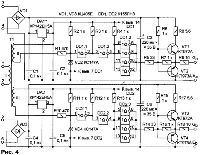
where UVD2 is the forward voltage drop across the diode VD2; W2 - number of turns of the secondary winding; Sc - cross section of the magnetic circuit; R - shunt resistance (R3-R8). Since the range of induction does not exceed the allowable value, the magnetic circuit is chosen correctly. CALCULATION OF THE TRANSFORMER OF GALVANIC Isolation On fig. 11 shows a diagram of a pulse shaper that controls the IGBT drivers of the output stage of the inverter. Five parallel-connected elements of the open-collector DD1 microcircuit serve to amplify the power of the control pulses. Resistor R3 limits the magnetizing current of transformer T1, the demagnetization circuit of the latter is formed by capacitor C3, diode VD2 and zener diode VD1.
The secondary windings of transformer T1 are loaded with inputs of TTL elements through 470 Ohm resistors (see Fig. 4), so the amplitude of the pulses taken from the windings should be 5 V at a current of approximately 10 mA. Since the amplitude of the pulses on the primary winding is 15 V, the required value of the transformation ratio is 3. The amplitude of the current pulse of the primary winding will be
With such a small current, the calculation of the diameter of the winding wire can be omitted, it gives values \u0,1b\u0,35bnot exceeding XNUMX mm. We choose the wire based on design considerations with a diameter of XNUMX mm. Conditional power of the transformer T1
By formula (3) we find
The filling factor of the magnetic circuit window ko is taken equal to 0,05 based on the need to provide good interwinding insulation. Let us choose for the transformer T1 a ring magnetic circuit K16x10x3 made of ferrite 2000NM1, in which Sc=0,09 cm2, So=0,785 cm2, ScSo=0,07 cm4. EMF of one turn wound on this magnetic circuit:
Number of turns of primary and secondary windings:
CONTROL BLOCK The control unit (CU) generates pulses that, through the driver (see Fig. 4), control the transistors of a forward single-cycle inverter. The set values of the welding current are regulated and maintained, while forming the falling external load characteristic of the IIST, which is optimal for welding, due to pulse-width modulation (PWM) - changing the duty cycle of the pulses. In the described control unit, the functions of protecting the source and its elements from overheating and overloads that occur under conditions of a sharply changing load are also implemented. The basis of the control unit - the SHI controller TDA4718A from Siemens - contains all the analog and digital components required for a switching power supply, and can be used to control push-pull transformer, half-bridge and bridge, as well as single-ended reverse and forward inverters. The internal structure of the TDA4718A controller is shown in fig. 12.
The voltage controlled oscillator (VCO) G1 generates pulses whose frequency depends on the voltage at its control input. The average value of the frequency change interval is set by choosing the values of the resistor RT and the capacitor St. The phase discriminator (PD) UI1 is used to synchronize the VCO with an external source of pulses. If synchronization is not required, the same VCO pulses are applied to the second input of the FD as to the first one, by connecting pins 5 and 14 of the microcircuit for this. The output of the FD is connected to the control input of the VCO and pin 17 of the microcircuit. An external filter capacitor Cf is connected to the latter. The sawtooth voltage generator (VPN) G2 triggers the VCO pulses. The sawtooth voltage is fed to the inverting input of comparator A1. The slope of the "saw" depends on the capacitance of the capacitor CR and the current in the output circuit 2 of the microcircuit. The ability to control the slope can be used, for example, to compensate for the instability of the supply voltage. Each pulse of the VCO sets the trip trigger D2 to a log state. 1 at the output, thus allowing the opening of transistors VT1 and VT2. However, only one of them can open each time, since the counting flip-flop D1 on the decay of the VCO pulses changes state. The output signals of comparators A1 or A6 reset the trigger D2, which leads to the closing of the open transistor. Comparator A1 has one inverting and (unlike conventional comparators) two non-inverting inputs. As soon as the instantaneous value of the "saw" at the inverting input exceeds the smallest of the voltage levels applied to the non-inverting inputs, the signal from the comparator output resets trigger D2. Thus, the duration of the pulses at the outputs of the SHI controller depends on the voltage applied to pin 4 of the microcircuit - one of the non-inverting inputs of comparator A1. The second non-inverting input of this comparator is involved in the controller's slow ("soft") start system. After the power is turned on, the capacitor Css is discharged and is charged by a current of 15 μA flowing from pin 6. The lower level of the sawtooth voltage at the inverting input of the comparator A1 is 1,8 V. Starting from this voltage value at the capacitor Css, pulses appear at the output of the comparator. As the capacitor charges, their duration, and with it the duration of the open state of transistors VT1, VT2, increases. As soon as the voltage on the capacitor Css exceeded the voltage applied to the second non-inverting input of the comparator, the "soft" start is completed, then the duration of the pulses depends on the voltage at pin 4 of the microcircuit. Comparator A2 is turned on in such a way that it limits the voltage on the capacitor Css to 5 V. Since the voltage at the output of the GPN can reach 5,5 V, by setting the appropriate "saw" slope, you can set the maximum duration of the open state of the output transistors of the controller. If the logic level at the output of trigger D3 is low (an error is fixed), the opening of the output transistors of the controller is prohibited, and the capacitor Css is discharged by a current of 15 μA flowing into pin 2. After some time, when the voltage on the capacitor Css drops to the threshold of the comparator A3 (1,5 V), the trigger D3 will receive a high output signal. But the flip-flop will be able to enter this state only if the levels at all four of its R inputs are high. This feature allows you to keep transistors VT1 and VT2 closed until all causes of controller blocking are eliminated. Comparators A4-A7 serve as error sensors, as well as a load current sensor built into the U1 exemplary voltage stabilizer with a response threshold of 10 mA. Comparators A4 and A5 give signals that turn trigger D3 into an error state if the voltage at the input of the first (pin 7) is higher, and at the input of the second (pin 6) is lower than the reference voltage generated by the stabilizer U1 of 2,5 V. Comparator A7 is triggered when the voltage drops power supply of the microcircuit up to 10,5 V. To fix the error, it is enough to operate one of the named comparators. Comparator A6 occupies a special position. It is designed to dynamically limit the current in inverter circuits. Both inputs of the comparator are connected to the external pins of the microcircuit, and its output is connected to the reset input of the trigger D2. The operation of the comparator A6 leads to the immediate closing of the currently open output transistor, and the normal mode will be restored (subject to the elimination of the cause of the protection operation) with the next VCO pulse without a "soft" start. The BU scheme is shown in fig. 13.
The nodes of the current sensor (see Fig. 10) and the output pulse shaper (see Fig. 11) considered earlier are not shown on it. Only one of the two outputs of the DA5 SHI controller is involved in the control unit. Since the controller is push-pull, the duty cycle of pulses at one output under no circumstances exceeds 0,5, which is required for the normal operation of a single-cycle inverter. To power the control unit, two windings of the transformer T1 (see Fig. 1) for a voltage of 20 V each were used. The alternating voltage from winding II is supplied to the diode bridge VD1, and the negative voltage rectified and smoothed by capacitor C1 is fed to the input of the stabilizer DA1, from the output of which a stabilized voltage of -15 V is removed to power the CU microcircuits. A voltage multiplier on diodes VD3-VD6 is connected to the same winding II , which gives an unregulated voltage of 100 V supplied to the welding circuit when the arc is not lit. The alternating voltage from the winding III of the transformer T1 (see Fig. 1) through the filter L2L3C29C30, which protects against impulse noise, is fed to the diode bridge VD26 and then through the diode VD27 to the stabilizer DA6. A voltage of 15 V is removed from the output of the latter to power the CU microcircuits, it also serves as an input for the DA7 stabilizer, with a voltage of 5 V from the output of which the TTL microcircuit of the output pulse shaper is fed (see Fig. 11). The voltage rectified by the VD26 bridge is applied through a voltage divider to resistors R45-R48 and to the inputs of comparators A4 and A5 of the DA5 controller. This ensures blocking of the IIST when the mains voltage goes beyond the permissible limits. By adjusting the tuning resistor R48, it is ensured that it occurs when the voltage goes out of the range of 205 ... 242 V. Capacitors C24 and C25 serve as additional protection against impulse noise. The comparator on the op-amp DA2.1 compares the voltage on the "soft" start capacitor C26 with the exemplary one at pin 10 of the controller. If the controller is in working condition, the voltage on the capacitor is greater than the reference voltage (2,5 V), the transistor VT2.1 is closed with a negative voltage from the output of the op-amp DA3, the HL1 LED (see Fig. 1) is off. Otherwise, the comparator DA2.1 goes into a stable state, thanks to positive feedback through the resistor R15 and diode VD14, with a positive voltage at the output, opening the transistor VT3. The HL1 LED that lights up (see Fig. 1) indicates that the IIST has stopped working due to the mains voltage going beyond the permissible limits. At the moment the IIST is connected to the network, the node on the op-amp DA2.2 generates a negative pulse that arrives at the non-inverting input of the op-amp DA2.1 and prohibits the alarm until the transients are completed and the inverter "soft" starts. A voltage of 10 V at the output of the DA8 stabilizer is set with a trimming resistor R62. The voltage is supplied to the input of this stabilizer through three resistors R55-R57 connected in parallel. The voltage drop across them is proportional to the current consumed by the stabilizer and its load. If its value is less than approximately 7 mA, the voltage at the output of the op-amp DA4.2 becomes negative, which leads to a decrease to zero (thanks to the diodes VD30, VD31) at pin 4 of the DA5 SHI controller and blocking the latter. Thus, the connection to the IIST of a remote control panel is controlled, which allows you to adjust the welding current from the welder's workplace. If the remote control is not connected or is faulty, a decrease of 5 mA in the current consumed through the 10 V circuit, caused by the disconnection of the variable resistor R2 (see Fig. 1), will not be compensated by the current consumed by the remote control, which will lead to the protection operation. Switch S1 is shown in the diagram for a better understanding of the operation of the device. It conditionally replaces the contacts of the relay control unit located outside the board, which switches the IIST to remote control. The voltage from the output of the current sensor (see Fig. 10) through the R43C21 filter is fed to pin 8 of the DA5 controller - one of the inputs of its comparator A6. A voltage of 9 V is supplied to the second input of the comparator (pin 38) from the R40R1,7 resistive divider. The dynamic current protection is triggered after the current of the inverter transistors exceeds 45 A. On the OS DA3.4, a node of the current protection drive is assembled. The voltage divider R25VD19R26 sets the threshold for its operation, corresponding to the current of the inverter power transistors of approximately 50 A. Until this value is exceeded, the diode VD21 is open, the voltage at the inverting input of the op-amp DA3.4 and capacitor C15 is equal to the threshold. Diodes VD20 and VD24 are closed, and the drive does not have any effect on the operation of the IIST. If the threshold is exceeded at the output of the op-amp DA3.4, a negative pulse will be generated, which will partially discharge the capacitor C34 through the resistor R16. The pulse duration depends on the time constant of the R32C15 circuit. If current overloads follow too often, the capacitor C16 will be discharged so much that the VD24 diode will open. This will reduce the voltage at pin 9 of the DA5 controller and temporarily lower the threshold for the dynamic current protection. In addition to the current protection unit, the voltage from the output of the current sensor of the power transistors of the inverter (see Fig. 10) is fed into the system for regulating and stabilizing the welding current. Through an inverting amplifier on the op-amp DA3.1, the VD16C13 circuit and the resistor R22, it enters the input of the DA3.2 op-amp and here it is algebraically summed with the variable resistor R2 coming from the engine (see Fig. 1) or the remote control. The amplified op-amp DA3.2 error signal through an inverting follower on the op-amp DA3.3, a voltage divider R28R29 and a VD22 diode is applied to terminal 4 of the DA5 controller - the input of its comparator A1. The VD17 zener diode does not allow positive voltage values at the output of the op-amp DA3.2, and limits the negative ones at the level of -10 V. Using the trimmer resistor R37, a voltage of 4 V is set at pin 5 of the DA1,8 controller, corresponding to the minimum duration of the output pulses. Trimmer resistors R42 and R44 regulate the frequency and duty cycle of the pulses of the SHI controller. The node on the op-amp DA4.1 automatically increases the frequency when the welding current is less than 25 ... 30 A in order to prevent interruption of the current in the welding circuit. This makes it possible to reduce the inductance and, consequently, the size and mass of the inductor L1 (see Fig. 1). The frequency is increased by applying additional current through the Zener diode VD23, resistor R39 and diode VD25 to the frequency setting circuit of the DA5 controller. If no measures are taken, in the absence of a load (when the arc is extinguished), the voltage at the IIST output, as a result of the influence of the parasitic inductance of the transformer and installation, can increase to a dangerous value. Therefore, the inverter part of the IIST is turned off in this mode, and the "standby" voltage from the above-mentioned multiplier on the VD1-VD2 diodes is applied to the welding electrodes through the resistor R3 and the diode VD6. While the voltage in the welding circuit exceeds the total stabilization voltage of the zener diodes VD8 and VD9, the transistor VT1 is open and shunts the LED of the optocoupler U1. The optocoupler transistor is closed, and VT2 is open and maintains (through the VD13 diode) almost zero voltage at pin 4 of the DA5 SHI controller, blocking the latter. When the welding electrodes are closed, the voltage between them drops, as a result, the transistor VT1, having closed, allows the current to flow through the LED of the optocoupler U1. The resulting opening of the transistor of the optocoupler U1 leads to the closing of the transistor VT2 and the diode VD13. In this state, the PWM controller operates normally until the voltage between the welding electrodes again exceeds approximately 40 V and the PWM controller is disabled again. This occurs at the end of the welding session as a result of a significant increase in the length of the arc gap. Forced extinction of the arc limits its maximum length, while eliminating the need for an excessive increase in the output power of the IIST. The temperature regime of powerful inverter transistors is controlled using a temperature-to-current converter VK1 mounted on their heat sink (see Fig. 1). A voltage proportional to the temperature of the heat sink is removed from the resistor R67 and fed to two comparators - op-amp DA4.3 and DA4.4. Capacitor C38 filters noise. The thresholds for the operation of the comparators are set by a resistive voltage divider R64, R69-R71. When the threshold corresponding to a temperature of +50 ° C is exceeded, the negative voltage from the output of the op-amp DA4.4 through the resistor R73 opens the transistor VT4. Relay K2 (see Fig. 1) is activated, turning on the block fan. If the temperature continues to rise and reaches +85 °C, the negative voltage already from the output of the op-amp DA4.3 through the VD18 diode enters the welding current control circuit, reducing it to 5 A. After the transistors and their heat sink cool down, the normal operation of the IIST will be automatically restored. The magnetic circuits of the L1-L3 chokes are ferrite rings with an outer diameter of 10 mm with an initial magnetic permeability of 1000 ... 2000. The windings are wound in one layer turn to turn with a conventional insulated mounting wire with a cross section of 0,1 mm2. Literature
Author: V.Volodin, Odessa, Ukraine
Air trap for insects
01.05.2024 The threat of space debris to the Earth's magnetic field
01.05.2024 Solidification of bulk substances
30.04.2024
▪ Smartphone Gigabyte GSmart GX2 ▪ Explosives will improve the safety of electric cars ▪ Humble Motors Humble One Solar Powered SUV ▪ NCP693 - new low power LDO regulator
▪ radio section of the website. Article selection ▪ article by Erich Fromm. Famous aphorisms ▪ Dagus article. Legends, cultivation, methods of application ▪ article Friendly aces. Focus secret
Comments on the article: a guest Very nice article, thanks. Victor Very well! Very good presentation! I'll take it on board. Thanks a lot.
Home page | Library | Articles | Website map | Site Reviews
www.diagram.com.ua |


 Leave your comment on this article: