|
|


 Arabic
 Bengali
 Chinese
 English
 French
 German
 Hebrew
 Hindi
Hindi Italian
 Japanese
 Korean
 Malay
Malay Polish
 Portuguese
 Spanish
 Turkish
 Ukrainian
 Vietnamese
|
ENCYCLOPEDIA OF RADIO ELECTRONICS AND ELECTRICAL ENGINEERING Transistor Voltage Regulators with Overload Protection
Encyclopedia of radio electronics and electrical engineering / Surge Protectors It seems that everything has been written about continuous voltage stabilizers. Nevertheless, the development of a reliable and not too complicated (no more than three or four transistors) stabilizer, especially with an increased load current, is a rather serious task, because one of the first places is the requirement of reliable protection of control transistors from overload. At the same time, it is desirable that after the elimination of the cause of the overload, the normal operation of the stabilizer is restored automatically. The desire to fulfill these requirements often leads to a significant complication of the stabilizer circuit and a noticeable decrease in its efficiency. The author of the proposed article is trying to find the optimal, in his opinion, solution. Before looking for the optimal solution, let's analyze the load characteristics Uout = f(Iout) of voltage stabilizers made according to the most common schemes. For the stabilizer described in [1], when overloaded, the output voltage Uout quickly drops to zero. However, the current does not decrease and can be sufficient to damage the load, and the power dissipated by the control transistor sometimes exceeds the allowable one. In [2], such a stabilizer is supplemented with trigger protection. When overloaded, not only the output voltage decreases, but also the current. However, the protection is not effective enough, since it works only after the output voltage drops below 1 V and, under certain conditions, does not eliminate the thermal overload of the regulating transistor. To return such a stabilizer to the operating mode, it is necessary to almost completely turn off the load, and this is not always acceptable, especially for a stabilizer that serves as an integral part of a more complex device. Protection of the stabilizer, the diagram of which is shown in fig. 1 is triggered already with a slight decrease in the output voltage caused by overload. The ratings of the circuit elements are given for an output voltage of 12 V in two versions: without brackets, if VD1 is D814B, and in brackets, if it is KS139E. A brief description of the operation of such a stabilizer is available in [3].
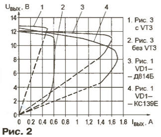
Its good parameters are explained by the fact that all the necessary signals are generated from a stabilized output voltage, and both transistors (regulating VT1 and control VT2) operate in the voltage amplification mode. The experimentally taken load characteristics of this stabilizer are shown in fig. 2 (curves 3 and 4).
When the output voltage deviates from the nominal value, its increment is transmitted almost completely through the zener diode VD1 to the emitter of the transistor VT2. If you do not take into account the differential resistance of the zener diode, ΔUe - ΔUout. This is a negative feedback signal. But the device also has a positive one. It is created by a part of the output voltage increment, supplied to the base of the transistor through the voltage divider R2R3:
The total feedback in the stabilization mode is negative, the error signal is the value
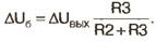
which is the greater in absolute value, the smaller R3 compared to R2. Reducing this ratio favorably affects the stabilization coefficient and the output resistance of the stabilizer. Given that
Zener diode VD1 should be selected for the maximum possible, but lower stabilization output voltage. If we replace the resistor R3 with two diodes connected in the forward direction and connected in series (as suggested, for example, in [4]), the stabilizer parameters will improve, since the place of R3 in the expressions for ΔUb and ΔUbe will be taken by a small differential resistance of open diodes. However, such a replacement leads to some problems when the stabilizer goes into protective mode. We will dwell on them below, but for now we will leave the resistor R3 in the same place. In the stabilization mode, the voltage drop across the resistor R1 remains almost unchanged. The current flowing through this resistor is the sum of the current of the zener diode VD1 and the emitter current of the transistor VT2, which is practically equal to the base current of the transistor VT1. With a decrease in load resistance, the last component of the current flowing through R1 increases, and the first (zener diode current) decreases down to zero, after which the output voltage increment is no longer transmitted to the emitter of transistor VT2 through the zener diode. As a result, the negative feedback circuit is broken, and the positive feedback that continues to operate leads to an avalanche closing of both transistors and cutoff of the load current. The load current, when exceeded, the protection is activated, can be estimated by the formula
where h21e is the current transfer coefficient of the transistor VT1. Unfortunately, h21e has a large variation from instance to instance of the transistor, depending on the current and temperature. Therefore, the resistor R1 often has to be selected when setting up. In a stabilizer designed for a large load current, the resistance of the resistor R1 is small. As a result, the current through the zener diode VD1, with a decrease in the load current, increases so much that it is necessary to use a high-power zener diode. The presence in the load characteristics (see curves 3 and 4 in Fig. 2) of relatively long transitional sections between the operating and protective modes (note that these sections are the most difficult in terms of the thermal regime of the transistor VT1) is mainly due to the fact that the development of the switching process prevents local negative feedback through resistor R1. The less voltage stabilization of the zener diode VD1, the greater, ceteris paribus, the value of the resistor R1 and the more "tightened" the transition from the working to the protective mode of the stabilizer. This, as previously made, the conclusion about the feasibility of using the Zener diode VD1 with the highest stabilization voltage possible is confirmed experimentally. The output voltage of the stabilizer according to the circuit shown in fig. 1, with a D814B zener diode (Ust = 9 V), compared to a similar KS139E zener diode (UCT = 3,9 V), it depends much less on the load and it more "coolly" switches to the protective mode when overloaded. It is possible to reduce and even completely eliminate the transition section of the load characteristic of the stabilizer by adding an additional transistor VT3 to it, as shown in Fig. 3.
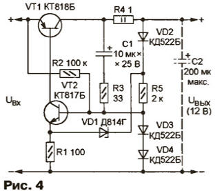
In operating mode, this transistor is in saturation and has practically no effect on the operation of the stabilizer, only slightly worsening the temperature stability of the output voltage. When, as a result of an overload, the current of the zener diode VD1 tends to zero, the transistor VT3 goes into the active state and then closes, creating the conditions for a quick turn on of the protection. There is no smooth transition section of the load characteristic in this case (see curve 1 in Fig. 2). Diodes VD2 and VD3 in the operating mode stabilize the voltage based on the transistor VT2, which improves the main parameters of the stabilizer. However, without an additional transistor VT3, this negatively affects the protection, as it weakens the positive component of the OS. Switching to the protective mode in this case is very delayed and occurs only after the voltage at the load drops to a value close to that supported by the diodes VD2 and VD3 based on the transistor VT2 (see curve 2 in Fig. 2). The considered stabilizers have a disadvantage that is significant for many applications: they remain in a protective state after the cause of the overload has been eliminated, and often do not go into operating mode when the supply voltage is applied with the load connected. There are various ways to start them, for example, using an additional resistor installed in parallel with the collector-emitter section of the transistor VT1, or (as proposed in [4]) "feeding" the base of the transistor VT2. The problem is solved by a compromise between the reliability of starting under load and the magnitude of the short circuit current, which is not always acceptable. The variants of launch units considered in [5] and [6] are more efficient, but complicate the stabilizer as a whole. An uncommon, but interesting way to bring the stabilizer out of the protection mode was proposed in [7]. It lies in the fact that a specially provided pulse generator periodically forcibly opens the regulating transistor, transferring the stabilizer to the operating mode for some time. If the cause of the overload is eliminated, at the end of the next pulse, the protection will not work again and the stabilizer will continue to operate normally. The average power dissipated in the control transistor during overload increases slightly. On fig. 4 shows a diagram of one of the possible options for a stabilizer operating on this principle. It differs from that described in [7] by the absence of a separate node - a pulse generator. When overloaded, the stabilizer goes into oscillatory mode due to the positive OS, which closes through the capacitor C1. Resistor R3 limits the charging current of the capacitor, and R4 serves as a generator load when an external load is closed.
In the absence of an overload, after applying the supply voltage, the stabilizer starts thanks to the resistor R2. Since the capacitor C1 is shunted by an open diode VD2 and resistors R3-R5 connected in series, the self-excitation conditions are not met and the device works similarly to that considered earlier (see Fig. 1). During the transition of the stabilizer to the protective mode, the capacitor C1 acts as a booster, accelerating the development of the process. The equivalent circuit of the stabilizer in protective mode is shown in fig. 5.
With a load resistance Rn equal to zero, the positive terminal of the capacitor C1 is connected through a resistor R4 to a common wire (minus the input voltage source). The voltage to which the capacitor was charged even in the stabilization mode is applied to the base of the transistor VT2 in negative polarity and keeps the transistor closed. The capacitor is discharged by current i1. current through resistors R3-R5 and an open diode VD2. When the voltage at the base of VT1 exceeds -0,7 V, the VD2 diode will close, but the capacitor will continue to recharge with the current i2 flowing through the resistor R2. Upon reaching a small positive voltage at the base of the transistor VT2, the latter, and with it VT1, will begin to open. Due to the positive feedback through the capacitor C1, both transistors will open completely and remain in this state for some time until the capacitor is charged with current i3 almost to the voltage Uin, after which the transistors will close and the cycle will repeat. With the diagram shown in Fig. 5 denominations of the elements, the duration of the generated pulses is units of milliseconds, the repetition period is 100 ... 200 ms. The amplitude of the output current pulses in the protective mode is approximately equal to the protection operation current. The average value of the short circuit current, measured with a pointer milliammeter, is approximately 30 mA. With an increase in load resistance RH, there comes a moment when, with open transistors VT1 and VT2, the negative OS "outweighs" the positive one and the generator again turns into a voltage stabilizer. The value of RH, at which the regime changes, depends mainly on the resistance of the resistor R3. If its values are too small (less than 5 ohms), hysteresis appears in the load characteristic, and at zero resistance R3, voltage stabilization is restored only when the load resistance is more than 200 ohms. An excessive increase in the resistance of the resistor R3 leads to the fact that a transition section appears in the load characteristic. The amplitude of negative polarity pulses based on transistor VT2 reaches 10 V, which can lead to electrical breakdown of the base-emitter section of this transistor. However, the breakdown is reversible, and its current is limited by resistors R1 and R3. It does not interfere with the operation of the generator. When choosing a transistor VT2, it is also necessary to take into account that the voltage applied to its collector-base section reaches the sum of the input and output voltages of the stabilizer. In operating equipment, the voltage regulator output is usually shunted by a capacitor (C2, shown in Fig. 4 by a dashed line). Its capacitance should not exceed 200 microfarads. The limitation is due to the fact that during an overload that is not accompanied by a complete closure of the output, this capacitor enters the positive feedback circuit of the generator. In practice, this is expressed in the fact that the generator "starts" only with a significant overload, and a hysteresis appears in the load characteristic. The resistance of the resistor R4 must be such that the voltage drop across it during the pulse is sufficient to open the transistor VT2 (-1 V) and ensure the conditions for self-generation at zero load resistance. Unfortunately, in stabilization mode, this resistor only reduces the efficiency of the device. For accurate operation of the protection, it is necessary that at any allowable load current, the minimum (taking into account ripples) input voltage of the stabilizer remains sufficient for its normal operation. When checking all the stabilizers discussed above with a rated output voltage of 12 V, a 14 V bridge diode rectifier with a 10000 microfarad capacitor at the output served as a power source. The ripple voltage at the rectifier output, measured with a VZ 38 millivoltmeter, did not exceed 0,6 V. If necessary, the impulse nature of protection can be used to indicate the state of the stabilizer, including sound. In the latter case, during overload, clicks will be heard with a pulse repetition rate. On fig. Figure 6 shows a diagram of a more complex stabilizer with impulse protection, largely devoid of the shortcomings discussed in the first part of the article (see Figure 4). Its output voltage is 12 V, output resistance is 0,08 Ohm, stabilization factor is 250, maximum operating current is 3 A, protection threshold is 3,2 A, average load current in protective mode is 60 mA. The presence of an amplifier on the VT2 transistor allows, if necessary, to significantly increase the operating current by replacing the VT1 transistor with a more powerful composite one.
The protection algorithm of this stabilizer differs little from the previously described one. In protective mode, transistors VT2 and VT3 form a pulse generator with a frequency-setting capacitor C1. Capacitor C2 suppresses high frequency parasitic generation. There is no serial resistor that degrades the efficiency in the output circuit of the stabilizer (similar to R4, see Fig. 4), the generator load is resistor R1. The purpose of the diodes VD1, VD2 and the transistor VT4 is similar to the elements VD2, VD3 and VT3 in the stabilizer according to the circuit shown in fig. 3. The value of the limiting resistor R4 can be in the range from tens of ohms to 51 kOhm. The output of the stabilizer can be shunted with a capacitor with a capacity of up to 1000 μF, which, however, leads to the appearance of hysteresis in the load characteristic: at a protection threshold of 3,2 A, the measured value of the return current to the stabilization mode is 1,9 A. For a clear switching of modes, it is necessary that with a decrease in load resistance, the current through the zener diode VD3 stops before the transistor VT2 enters saturation. Therefore, the value of the resistor R1 is chosen in such a way that before the protection trips between the collector and emitter of this transistor, a voltage of at least 2 remains ... 3 V. In the protective mode, the transistor VT2 enters saturation, as a result, the amplitude of the load current pulses can be 1.2 ... 1,5 times the protection operation current. It should be borne in mind that with a significant decrease in the resistance R1, the power dissipated on the transistor VT2 increases significantly. The presence of capacitor C1 can theoretically lead to an increase in the output voltage ripple of the stabilizer. However, this has not been observed in practice. The output stabilized voltage is equal to the sum of the voltage drops across the diodes VD1 and VD2, the base-emitter section of the VT4 transistor and the stabilization voltage of the VD3 zener diode, minus the voltage drop in the base-emitter section of the VT3 transistor - approximately 1,4 V more than the stabilization voltage of the zener diode. The protection trip current is calculated by the formula
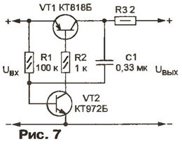
Thanks to an additional amplifier on the transistor VT2, the current flowing through the resistor R3 is relatively small, even with significant rated load currents. This, on the one hand, improves the efficiency of the stabilizer, but on the other hand, it forces the use of a zener diode capable of operating at low currents as VD3. The minimum stabilization current shown in the diagram (see Fig. 6) of the KS211Zh zener diode is 0,5 mA. Such a stabilizer, in addition to its direct purpose, can serve as a battery discharge limiter. To do this, the output voltage is set so that when the battery voltage is less than the allowable one, the protection will work, preventing further discharge. The value of the resistor R6 in this case, it is advisable to increase to 10 kOhm. As a result, the current consumed by the device in operating mode will decrease from 12 to 2,5 mA. It should be borne in mind that on the verge of protection operation, this current increases to approximately 60 mA, but with the start of the pulse generator, the average value of the battery discharge current drops to 4 ... 6 mA. According to the considered principle of impulse protection, it is possible to build not only voltage stabilizers, but also self-healing electronic "fuses" installed between the power source and the load. Unlike fusible links, such fuses can be used repeatedly without worrying about recovery after the cause of operation has been eliminated. The electronic fuse must withstand both short-term and long-term, full or partial load closure. The latter often occurs with long connecting wires, the resistance of which is a significant part of the payload. This case is the most difficult for the switching element of the fuse. On fig. 7 shows a diagram of a simple self-healing electronic fuse with impulse protection. The principle of its operation is close to the voltage stabilizer described above (see Fig. 4), but before the protection is activated, transistors VT1 and VT2 are in saturation and the output voltage is almost equal to the input.
If the load current has exceeded the allowable value, the transistor VT1 comes out of saturation and the output voltage begins to decrease. Its increment through the capacitor C1 enters the base of the transistor VT2, closing the latter, and with it VT1. The output voltage decreases even more, and as a result of the avalanche process, the transistors VT1 and VT2 are completely closed. After some time, depending on the time constant of the R1C1 circuits, they will open again, however, if the overload persists, they will close again. This cycle is repeated until the overload is removed. The frequency of the generated pulses is approximately 20 Hz when the load is slightly higher than the permissible one, and 200 Hz when it is completely closed. The duty cycle of the pulses in the latter case is more than 100. When the load resistance increases to an acceptable value, the transistor VT1 will enter saturation and the generation of pulses will stop. The operating current of the "fuse" can be approximately determined by the formula
The coefficient of 0,25, selected experimentally, takes into account that at the moment of transition of the transistor VT1 from saturation to the active mode, its current transfer coefficient is much less than the nominal one. The measured current of the protection operation at an input voltage of 12 V is 0,35 A, the amplitude of the load current pulses when it is closed is 1,3 A. The hysteresis (the difference between the currents of the protection operation and restoration of the operating mode) was not detected. If necessary, blocking capacitors with a total capacity of not more than 200 microfarads can be connected to the "fuse" output, which will increase the trip current to approximately 0,5 A. If it is necessary to limit the amplitude of the load current pulses in the emitter circuit of the transistor VT2, a resistor of several tens of ohms should be included and the value of the resistor R3 should be slightly increased. If the load is not completely closed, electrical breakdown of the base-emitter section of the transistor VT2 is possible. This affects the operation of the generator insignificantly, and it does not pose a danger to the transistor, since the charge accumulated in the capacitor C1 before the breakdown is relatively small. The disadvantages of the "fuse" assembled according to the considered scheme (Fig. 7) are low efficiency due to the resistor R3 connected in series in the load circuit and the base current of the transistor VT1, which is independent of the load. The latter is typical for other similar devices [8]. Both reasons that reduce efficiency are eliminated in a more powerful "fuse" with a maximum load current of 5 A, the circuit of which is shown in fig. 8. Its efficiency exceeds 90% in more than ten times the change in load current. The current consumed in the absence of load is less than 0,5 mA.
To reduce the voltage drop across the "fuse", a germanium transistor is used as VT4. When the load current is less than the allowable, this transistor is on the verge of saturation. This state is supported by a negative feedback loop, which, when the transistor VT2 is open and saturated, is formed by transistors VT1 and VT3. The voltage drop in the collector-emitter section of the transistor VT4 does not exceed 0,5 V at a load current of 1 A and 0,6 V at 5 A. When the load current is less than the protection trip current, the transistor VT3 is in active mode and the voltage between its collector and emitter is sufficient to open the transistor VT6, which ensures the saturated state of the transistor VT2 and, ultimately, the conductive state of the key VT4. With an increase in the load current, the base current VT3 under the influence of a negative OS increases, and the voltage on its collector decreases until the transistor VT6 closes. At this moment, the protection kicks in. The tripping current can be estimated by the formula
where Req is the total resistance of resistors R4, R6 and R8 connected in parallel. The coefficient 0,5, as in the previous case, is experimental. When the load is closed, the amplitude of the output current pulses is approximately twice the current of the protection operation. Due to the action of the positive OS, which closes through the capacitor C2, the transistor VT6, and with it VT2-VT4, are completely closed, VT5 opens. The transistors remain in the indicated states until the charging of the capacitor C2 is completed by the current flowing through the base-emitter section of the transistor VT5 and resistors R7, R9, R11, R12. Since R12 has the largest value of the listed resistors, it determines the repetition period of the generated pulses - approximately 2,5 s. After the charging of the capacitor C2 is completed, the transistor VT5 will close, VT6 and VT2-VT4 will open. Capacitor C2 is discharged in approximately 0,06 s through transistor VT6, diode VD1 and resistor R11. With a closed load, the collector current of the transistor VT4 at this time reaches 8 ... 10 A. Then the cycle will repeat. However, during the first pulse after the overload is eliminated, the transistor VT3 will not enter saturation and the "fuse" will return to operating mode. Interestingly, during the pulse, the transistor VT6 does not open completely. This is prevented by the negative OS loop formed by transistors VT2, VT3, VT6. With the value of the resistor R8 (9 kOhm) indicated in the diagram (Fig. 51), the voltage at the collector of the transistor VT6 does not drop below 0,3 Uin. The most unfavorable load for the "fuse" is a powerful incandescent lamp, in which the resistance of a cold filament is several times less than that of a heated one. A test carried out with a 12 V 32 + 6 W car lamp showed that 0,06 s for warming up is quite enough and the "fuse" after it is turned on reliably enters the operating mode. But for more inertial lamps, the duration and repetition period of the pulses may have to be increased by installing a larger capacitor C2 (but not oxide). The duty cycle of the generated pulses as a result of such a replacement will remain the same. Equal to 40, it was not chosen by chance. In this case, both at the maximum load current (5 A) and when the "fuse" output is closed, approximately the same and safe power is dissipated on the VT4 transistor. The GT806A transistor can be replaced with another from the same series or a powerful germanium one, for example, P210 with any letter index. If there are no germanium transistors or it is necessary to work at elevated temperatures, silicon transistors with h21e> 40 can also be used, for example, KT818 or KT8101 with any letter indices, increasing the value of the resistor R5 to 10 kOhm. After such a replacement, the voltage measured between the collector and emitter of the VT4 transistor did not exceed 0,8 V at a load current of 5 A. When making a "fuse", the VT4 transistor must be installed on a heat sink, for example, an aluminum plate with dimensions of 80x50x5 mm. A heat sink with an area of 1,5 ... 2 cm2 is also needed for the VT3 transistor. Turn on the device for the first time without load, and first of all, check the voltage between the collector and emitter of the VT4 transistor, which should be approximately 0,5 V. Then connect a wire variable resistor with a resistance of 10 ... 20 Ohm and a power of 100 W to the output through an ammeter. Gradually decreasing its resistance, put the device into protection mode. Using an oscilloscope, make sure that the mode switching occurs without prolonged transients, and the parameters of the generated pulses correspond to those indicated above. The exact value of the protection operation current can be set by a selection of resistors R4, R6, R8 (it is desirable that their ratings remain the same). With a prolonged load circuit, the temperature of the case of the transistor VT4 should not exceed the value allowed for it. Literature
Author: A. Moskvin, Yekaterinburg
Artificial leather for touch emulation
15.04.2024 Petgugu Global cat litter
15.04.2024 The attractiveness of caring men
14.04.2024
▪ Nanosheets instead of platinum ▪ Marital status of a person and his state of health ▪ Ford cars will learn to track free parking lots ▪ Portable devices harm the development of speech
▪ section of the site Metal detectors. Article selection ▪ article Time heals wounds. Time is the best doctor, medicine. Popular expression ▪ article Is it possible to shoot nuclear shells from artillery mounts? Detailed answer ▪ article Machinist grit sprayer. Standard instruction on labor protection ▪ article Simple ignition switch. Encyclopedia of radio electronics and electrical engineering
Comments on the article: Gennady Many thanks for the article and ATTENTION to the person !!!
Home page | Library | Articles | Website map | Site Reviews
www.diagram.com.ua |


 Leave your comment on this article: