|
|


 Arabic
 Bengali
 Chinese
 English
 French
 German
 Hebrew
 Hindi
Hindi Italian
 Japanese
 Korean
 Malay
Malay Polish
 Portuguese
 Spanish
 Turkish
 Ukrainian
 Vietnamese
|
ENCYCLOPEDIA OF RADIO ELECTRONICS AND ELECTRICAL ENGINEERING Half-bridge quasi-resonant power supply. Encyclopedia of radio electronics and electrical engineering
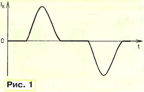
Encyclopedia of radio electronics and electrical engineering / Power Supplies To improve the characteristics of switching power supplies assembled on the basis of bridge and half-bridge converters, in particular, to reduce the likelihood of a through current and increase the efficiency, the authors propose to transfer such sources to a quasi-resonant mode of operation. The described article provides a practical example of such a power supply. Often, to reduce the size and weight, power supplies (PS) with a network transformer are replaced by pulse voltage converters. The benefit from this is obvious: smaller weight and dimensions, significantly lower copper consumption for winding products, high efficiency of the IP. However, pulsed power supplies also have disadvantages: poor electromagnetic compatibility, the possibility of through current through transistors in push-pull converters, the need to introduce overcurrent protection circuits, the difficulty of starting on a capacitive load without taking special measures to limit the charging current. Consider, using the example of a push-pull half-bridge autogenerator voltage converter [1], how to a certain extent it is possible to eliminate or reduce these shortcomings by changing its mode of operation. Let's translate the converter into a quasi-resonant mode of operation by introducing a resonant circuit [2]. The shape of the current through the primary winding of the pulse transformer in this case is shown in fig. 1.
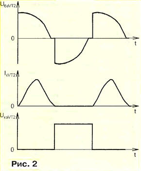
On fig. 2 shows the voltage and current waveforms for one of the switching transistors. It can be seen from the figures that the converter operates in a quasi-resonant mode - there is no through current in this case.
The voltage at the base of the switching transistor decreases and by the end of the pulse becomes equal to zero. Thus, the transition to a quasi-resonant mode of operation completely eliminates the dynamic losses in switching transistors and the problems associated with the electromagnetic compatibility of sensitive devices with a pulsed MT, since the spectrum of generated oscillations is sharply narrowed. A half-bridge converter differs from a push-pull bridge in a smaller number of transistors used; from a push-pull with an average output - half the voltage on the transistors. A self-oscillating converter differs from converters with a master oscillator, first of all, by the minimum number of elements, the maximum possible efficiency, and the use of a saturable auxiliary transformer is guaranteed to exclude the possibility of a through current. The scheme of a half-bridge quasi-resonant IP, devoid of the above disadvantages, is shown in Fig. 3.
Main Specifications
The power supply contains the following nodes: S1C2L1 noise suppression filter, which prevents high-frequency ripples generated by the converter from penetrating into the supply network; mains rectifier VD1 with filter capacitor C3; protection circuits against overload and short circuits in the load R1R2VD2K1U1VD3VD4R6R7C7. The protection circuit consumes a small current, so it has little effect on the overall efficiency of the source, but if necessary, the efficiency can be slightly increased by replacing the VD2 zener diode with a higher voltage one. Resistors R6 and R7 form the voltage divider required to turn on the emitting diode of the thyristor optocoupler. If these fixed resistors are replaced by a single variable, it is possible to adjust the protection response threshold over a very wide range. If it is planned to power a load with a large capacitance (more than 5000 microfarads), in order to avoid false alarms of the protection, the capacitance of the capacitor C7 should be increased, but the waiting time before the source is turned on will increase in this case. Elements R3, R4, C4, C5 form a voltage divider. Resistors R3, R4 are needed to discharge the filter capacitors C3 and divider C4C5 after the power supply is turned off. Capacitor C6 and inductor L2 - resonant circuit. The trigger circuit is exactly the same as in the device described in article [1]. It consists of a transistor VT3, resistors R10-R12 and capacitor C10. Transistor VT3 operates in avalanche mode. The trigger pulse opens the transistor VT2, providing the initial asymmetry. Diodes VD5-VD8 - output rectifier with filter capacitors C8, C9. LED HL1 indicates the presence of voltage at the output of the IP. Auto-generation of oscillations occurs as a result of the action of positive feedback from the winding III of the transformer T1 to the winding III of the transformer T2 through the current-limiting resistor R9. With a decrease in its resistance, the conversion frequency decreases, which leads to a shift in the maximum efficiency of the source towards a higher load power. The device uses capacitors K73-17 (C1, C2, C6, C9, C10), K73-11 (C4, C5), K50-32 (C3), K50-24 (C7, C8). All resistors are C2-23. Instead of the indicated capacitors and resistors, it is possible to use other components, however, capacitors should be selected with a minimum dielectric loss tangent in the operating frequency range of the IP conversion. Diode bridge VD1 - any with a permissible forward current of more than 1 A and a permissible reverse voltage of at least 400 V, for example BR310. It is also possible to use discrete diodes, for example KD202R, connected in a bridge circuit. It is best to use the KT315G (VT3) transistor in the device - the trigger circuit will work with it immediately, the KT315B transistor will have to be selected, and it is better not to use the KT315A, KT315V transistors. Transistors KT826V (VT1, VT2) are replaceable by any of the KT826 or KT812A, KT812B series. Due to low losses, transistors can not be installed on heat sinks. Diodes of the output rectifier KD213A (VD5-VD8) can be replaced with KD213B, KD213V or KD2997, KD2999 series. They should be installed on a heat sink with a cooling surface area of at least 10 cm2. The IP uses a DC electromagnetic relay GBR10.1-11.24 with an operating voltage of 24 V, capable of switching an alternating current of 8 A in circuits with a voltage of up to 250 V. It can be replaced by any other with a permissible switched alternating current of at least 1 A in circuits with voltage 250 V. However, it is desirable to use a relay with a minimum switching current to increase the efficiency of the power supply, since the lower the operating current, the greater the resistance should have resistors R1, R2 and less power will be dissipated on them. Inductors L1, L2 and transformer T1 are used ready-made - from an old computer EC1060: L1 - I5, L2 - 4777026 or 009-01, T1 - 052-02. You can also make them yourself. Inductor L1 is wound (two windings at the same time) on a K28x16x9 annular magnetic circuit made of ferrite (for example, grades M2000NM-A or M2000NM1-17) or alsifer. Its windings contain 315 turns of PEV-2 0,3 wire. The resonant inductor L2 is wound on a K20x10x5 ring magnetic circuit made of M2000NM-A ferrite. Its winding contains 13 turns of PEV-2 0,6 wire. Transformer T1 is wound on a K45x28x8 ring magnetic circuit made of M2000NM1-17 ferrite. Winding I contains 200 turns of wire PEV-2 0,6, winding II - 35 turns of wire PEV-2 1, winding III - 5 turns of wire PEV-2 0,6. The order of winding the windings on the magnetic circuit is arbitrary. Between the windings it is necessary to lay a layer of insulation, for example, fluoroplastic tape. In addition, the transformer should be impregnated, for example, with candle paraffin or ceresin. This will not only increase the dielectric strength of the insulation, but also reduce the hum generated by the source at idle. Transformer T2 is wound on a K20x10x5 ring magnetic circuit made of M2000NM-A ferrite. Windings I and II contain seven turns of PEV-2 0,3 wire each (they are wound simultaneously in two wires), and winding III contains nine turns of PEV-2 0,3 wire. The design of the IP can be arbitrary, the relative position of the elements on the board is not critical. It is only important to ensure good air flow to the semiconductor devices by natural convection or install the power supply inside the powered device near the fan. The described IP practically does not need to be adjusted, although it is worth making sure that the converter operates in a quasi-resonant mode. To do this, a load equivalent is connected to the output of the power supply - a resistor with a power of 100 W and a resistance of 36 ohms. In series with capacitor C6, an additional resistor with a resistance of 0,1 ... 1 Ohm and a power of 1 ... 2 W is included. Oscilloscope probes are connected to an additional resistor: common - to the midpoint of the voltage divider R3R4C4C5, signal - to capacitor C6. You must make sure that the oscilloscope is not galvanically connected to the network. If connected, it should be connected to the network through an isolating transformer with a transformation ratio of 1:1. In any case, the safety regulations must be observed. Having applied power to the IP, they are convinced of the presence of bell-shaped current pulses with a pause at zero. If the pulse shape differs from that shown in Fig. 1, it is necessary to select the number of turns of the inductor L2 until resonance is obtained. On an additional resistor with a resistance of 0,1 Ohm, the amplitude of the pulses should be about 0,1 V. Now you should compare the shape of the current and voltage on the switching transistor VT2 with those shown in Fig. 2 charts. If they are close in shape, the IP operates in a quasi-resonant mode. The protection threshold can be changed. To do this, select the resistance of the resistor R7 so that the protection operates at the required load current. If it is necessary for the power supply to turn off when the power in the load is less than 70 W, the resistance of the resistor R7 should be reduced. To limit the charging current of the capacitor C3 at the time of switching on, we recommend connecting a resistor with a resistance of 5,6 ... 10 Ohm with a power of 2W to the break of any network wire. Literature
Authors: E. Gaino, E. Maskatov, Taganrog, Rostov region.
Machine for thinning flowers in gardens
02.05.2024 Advanced Infrared Microscope
02.05.2024 Air trap for insects
01.05.2024
▪ A unique method for studying genes has been developed ▪ How to recognize someone else's dream ▪ Weather does not affect mood ▪ Razer Ornata - the first keyboards with Razer Mecha-Membrane switches
▪ section of the site Voltage stabilizers. Article selection ▪ article by Ørsted Hans. Biography of a scientist ▪ article How and why did Ariadne help Theseus defeat the Minotaur? Detailed answer ▪ article Water turns into... blood. Focus secret
Comments on the article: Vladimir The scheme is very attractive. But there are a few questions: the operating frequency changes from 12 kHz to 57 kHz when the load changes. Therefore, the efficiency is also subject to change. At what load is the maximum frequency and at what minimum? Is it possible to use "our" Chinese radio components in the circuit? Transistors, capacitors and ferrites. The inductance of the resonant coil is not specified, but it would be nice. Otherwise, everything is clear and corresponds to working circuits with a resonant load. One last question: Is the fluorescent light ballast circuit resonant or quasi-resonant? I'm a little confused on the definitions. [oops] [up]
Home page | Library | Articles | Website map | Site Reviews
www.diagram.com.ua |


 Leave your comment on this article: