|
|


 Arabic
 Bengali
 Chinese
 English
 French
 German
 Hebrew
 Hindi
Hindi Italian
 Japanese
 Korean
 Malay
Malay Polish
 Portuguese
 Spanish
 Turkish
 Ukrainian
 Vietnamese
|
ENCYCLOPEDIA OF RADIO ELECTRONICS AND ELECTRICAL ENGINEERING Unusual mode of operation of the field-effect transistor. Encyclopedia of radio electronics and electrical engineering
Encyclopedia of radio electronics and electrical engineering / Radio amateur designer The traditional circuitry of linear amplifiers based on field-effect transistors with a gate in the form of a pn-junction (hereinafter referred to as a pn-gate for brevity) mainly provides for the mode when the operating point is in the region of the reverse (closing) bias, i.e. at Uots The studies conducted by the author have shown that the use of a mode in which the operating point can be in the zone of the opening bias can significantly simplify the circuits of nodes on field-effect transistors. The use of such schemes is rational in cases where the requirement for a minimum number of elements justifies the need to select some of them, i.e., in amateur radio practice and in the development of especially miniature designs.
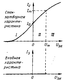
On fig. 1 shows the generalized drain-gate and input characteristics of a pn-gate FET. On these current-voltage characteristics - Iс=f(Uin) and Iz=f(Uin) - three characteristic zones can be distinguished: 1 - closing bias Uzi, 2 - opening bias, at which there is practically no gate current, and 3 - opening bias , which causes a significant gate current. There is no clear boundary between zones 2 and 3, therefore, for definiteness, we will take as a conditional boundary between them the ordinate corresponding to a gate current of 1 μA - at this current, the gate resistance is still very high, and this value can be relatively easily measured. We also denote the drain current at this boundary and the forward voltage at the gate Um by the symbol Im. At a voltage Uzi greater than the limit, the gate current begins to increase sharply and the field-effect transistor loses its main advantage - high input resistance. Therefore, work in zone 3 is not considered. From the foregoing, it is clear that there is no need to completely exclude the operation of the field-effect transistor in the forward bias zone, it is quite enough that the operating point does not go into zone 3, i.e., the condition Uzi Despite the fact that the expansion of the operating voltage range Uzi due to the addition of a forward bias zone is small in absolute value, it is very important, since it allows a slightly different approach to the circuitry of field-effect transistors. As can be seen from fig. 1, the drain-shutter characteristic passes into zone 2 smoothly, without a break. The essence of the physical processes in the transistor is that when a direct bias voltage is applied to the gate, the channel expands and its conductivity increases, the transistor starts to work in the enrichment mode. It is easy to see that, taking into account the forward bias zone, a pn-gate transistor becomes similar in characteristics to an insulated gate transistor with an integrated channel, which is capable of operating with forward and reverse bias on the gate. The difference is only quantitative - in the first of them, the working area of the direct displacement zone is shorter, since it is limited by the value of Um. Therefore, a pn-gate field-effect transistor can be used in modes that were considered possible only for transistors with an insulated gate and an integrated channel. The presence of serious shortcomings in transistors with an insulated gate - a significant spread of characteristics, low resistance to static electricity, and a number of others - sharply limits the scope of practical application of these devices, even if their individual selection is admissible. The range of currently produced transistors with a pn-gate is much wider than with an isolated one, they are more affordable and have a smaller spread of characteristics. For these reasons, pn-gate transistors should be considered more preferable.
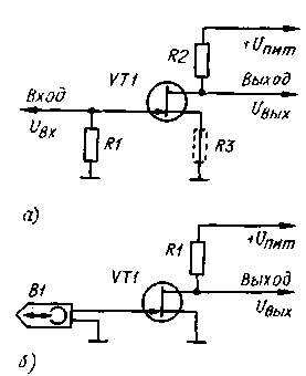
Let's look at some applications of these transistors using the gate forward bias mode. On fig. 2a shows a diagram of a linear amplifier. The use of an operating mode without an initial bias made it possible to eliminate the automatic bias resistor and the blocking capacitor in the source circuit of the transistor VT1. The calculation of the DC step is simplified and reduced to determining the resistance of the load resistor R2 using the formula: R2 \uXNUMXd (Upit-Uout o) / Io where Uout o is the output voltage in the absence of an input signal, and Io is the initial current of the transistor. When choosing Uout o= 0,5 Upit, formula (1) is simplified and takes the form: R2=Upit/2Io. When developing amplifiers according to this scheme, it should be borne in mind that for transistors with an initial drain current of several tens of milliamps, their allowable power may be exceeded. If it is necessary to reduce the gain, a resistor R3 is included in the source circuit. It should be emphasized that in this case the blocking capacitor cannot be switched on. The alternating current mode is calculated according to known formulas; the gain is found from the expression Ku \u2d S • R10, where S is the slope of the transistor characteristic. Obviously, at Ku>1,1, in most cases, the amplification of the output signal in amplitude up to Upit occurs at Uin If it is necessary to increase the allowable amplitude of the positive input voltage above Um, it is required to turn on the diode instead of the resistor R3 in the source circuit (cathode to the common wire). The forward bias voltage for silicon diodes can be in the range of 0,4 ... 0,8 V (in most cases 0,5 ... 0,7 V) depending on the type of diode and the source current of the transistor. For germanium diodes, similar values are 0,2 ... 0,6 V (0,3 ... 0,5 V). When the diode is turned on, the drain current decreases due to the closing bias, therefore, to ensure the previous DC mode, it is necessary to increase the resistance of the resistor R2. This, in turn, leads to an increase in Kn, since the steepness decreases slightly. Since the dynamic resistance of the diode is small, shunting it with a capacitor is ineffective. The introduction of a diode causes a small - no more than 10% - decrease in gain. The mode of such a stage for direct current is calculated by formula (1), in which instead of Io, Iod is substituted - the drain current with a diode connected to the source circuit. If necessary, Ku can be reduced by connecting a feedback resistor in series with the diode. Despite the presence of an additional diode, the implementation of such a circuit in some cases is justified for the reason that it leads to a decrease in current consumption and an increase in the gain. These properties are especially valuable for self-powered devices. As can be seen from the above, the operation of a stage with a diode is close to the classical one with a bias resistor. The main advantage is the absence of a blocking capacitor, which also leads to an expansion of the operating frequency band from below up to direct current. In addition, the calculation and adjustment of devices is simplified. When this stage is used with a transformer, coupling coil, tape recorder head and other similar signal sources, no leakage resistor R1 is required and the circuit takes the extremely simple form shown in Fig. 2b.
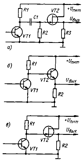
The possibility of operation of a field-effect transistor with a pn-gate under forward bias, discussed above, can also be effectively used to build another important class of devices - source followers. On fig. 3, and shows the traditional circuit of the source follower transistor VT2. The main disadvantage of this node is the relatively narrow limits of the output voltage. The traditional emitter follower (VT2, Fig. 3, b) is free from this disadvantage; in addition, it has fewer details. But the emitter follower has a relatively low input resistance: Rin = h21eRe (h21e is the static current transfer coefficient of the transistor; Re is the resistance of the resistor in the emitter circuit). All noted contradictions are completely eliminated with direct connection of the source follower, as shown in Fig. 3, c. Here, the advantages of the source and emitter followers are successfully combined. This scheme did not find practical application, apparently because it is impossible to avoid a forward bias voltage on the gate. But this is not required, it is enough to exclude the operation of the transistor in the region of the forward current of the gate (in zone 3 in Fig. 1). This problem is solved quite simply, which makes it possible to apply such a scheme in practice. The transfer characteristic of the source follower is determined by the general expression: Uout=Uo+UinxKp, (2) where Uo is the initial output voltage at Uin=0; Kp - transmission coefficient of the source follower. For the follower to operate in the region of the closing bias on the gate, it is necessary that the condition Uz In fact, the real requirements are less stringent, since it suffices to fulfill a simpler condition: U and Upit (Ri is the resistance of the resistor in the source circuit). Considering the tentative nature of the calculation according to this formula, the absence of the gate current at Uz = Upit should be checked when prototyping the node with a microammeter with a full deflection current of the arrow of not more than 100 μA. The output voltage of such a source follower is within Uo ... (Upit-Usi).
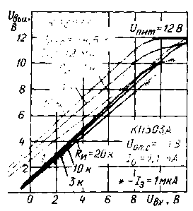
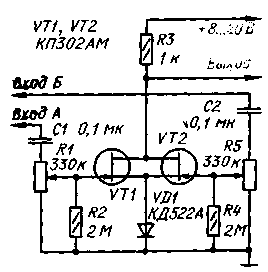
The dependences Uout=f(Uin) experimentally taken at Upit=12V for KPZOZA and KPZOZE transistors at different values of resistance Ri are shown in Fig. 4. As can be seen from the graphs, it is possible to ensure the linearity of the transfer characteristic in the range from Uout (at Uin = 0) to (Upit- -1) V. To expand this section, you should, first of all, reduce Uo, for which you need to use transistors with the minimum value of Uotc, and then select the optimal resistance of the resistor R and (R2 in the diagram in Fig. 3, c). An asterisk on the graphs marks the points where the current Iz reaches a value of 1 μA. As an example of the practical application of the described linear amplification mode in Fig. 5 shows a diagram of a two-channel 3H signal mixer; in general, the number of channels is not limited by anything and can be any. The resistance of the resistor R3 is determined by the formula (1), in which Iod n is substituted instead of Io, where n is the number of channels.
In the device, it is desirable to use transistors with close values of Uots and Io (or Iod), however, the spread of these parameters up to 50 ... 100% is quite acceptable, since the gain difference between the channels can be easily compensated by the input regulators R1, R5. Be sure to check that none of the channels entered the amplitude limiting mode in the operating range of the input voltage. When using a silicon diode, the permissible amplitude of the positive half-wave at the gate of each field-effect transistor is at least 1 V. When one channel is operating at supply voltage Upit=9 V, output voltage Uout=0,1 V (effective value), signal frequency fc=0,1 kHz, the mixer gain is approximately equal to 3, and in terms of the level of non-linear distortions it is not inferior to that built according to classical circuitry. Author: A. Mezhlumyan, Moscow; Publication: N. Bolshakov, rf.atnn.ru
A New Way to Control and Manipulate Optical Signals
05.05.2024 Primium Seneca keyboard
05.05.2024 The world's tallest astronomical observatory opened
04.05.2024
▪ Mechanical centipede for intestinal diagnostics ▪ Photon encrypts communication
▪ section of the site Signal limiters, compressors. Article selection ▪ article Flat sharpness. Popular expression ▪ article Installer of lifting and transport equipment of discontinuous action. Job description ▪ article Security device for the car. Encyclopedia of radio electronics and electrical engineering
Home page | Library | Articles | Website map | Site Reviews
www.diagram.com.ua |

 Leave your comment on this article: