|
|


 Arabic
 Bengali
 Chinese
 English
 French
 German
 Hebrew
 Hindi
Hindi Italian
 Japanese
 Korean
 Malay
Malay Polish
 Portuguese
 Spanish
 Turkish
 Ukrainian
 Vietnamese
|
ENCYCLOPEDIA OF RADIO ELECTRONICS AND ELECTRICAL ENGINEERING Acoustic light switch. Encyclopedia of radio electronics and electrical engineering
Encyclopedia of radio electronics and electrical engineering / Lighting The logic of the acoustic switch is similar to a counting trigger. An audible signal turns on the lamps if they are off, or off if they are on. In the pauses between signals, the state of the lamps remains unchanged.
The switch diagram is shown in fig. 1. EL1 - one or more lamps connected in parallel (incandescent or "energy saving") with a total power of up to 1000 W, controlled by a switch. Thanks to the use of economical microcircuits K154UD1A [1] and HEF4013BP [2], the active component of the current consumed from the network when the lamp is off is only 0,88 mA. As practice has shown, the inclusion of a lamp in a DC circuit rectified by a diode bridge VD1, and not alternating current, provides better noise immunity of the device. The voltage rectified by this bridge, after extinguishing its excess with resistor R7, limiting the zener diode VD4 at 10 V and smoothing with capacitor C1, is also used to power microcircuits. Capacitor C6 in their power circuit suppresses high-frequency interference. Due to the low current consumption, the power dissipated by the resistor R7 does not exceed 0,25 watts. Capacitor C3 significantly reduces the likelihood of false operation of the device switch from interference penetrating from the mains. This has been confirmed experimentally. Op-amp DA1 amplifies the signals coming from the BM1 microphone. The gain, on which the response threshold depends, is adjusted by the trimming resistor R4. Since the connection of the inverting input of the op-amp with a common DC wire is broken by capacitor C4, the constant component of the voltage at this input and at the output of the op-amp is always equal to the same voltage component at the non-inverting input of the op-amp. By selecting the resistor R1 in the power supply circuit of the BM1 microphone, it is set approximately equal to half the supply voltage of the op-amp. This makes it possible to obtain the maximum swing of the AC voltage at its output. Capacitors C2 and C5 form the frequency response of the amplifier, suppressing the high-frequency components of the signal. An amplitude detector of the variable component of the signal is assembled on diodes VD2 and VD3. Resistor R5 slows down the rise in voltage across capacitor C8, preventing the switch from tripping from too short acoustic signals. Through resistor R6, capacitor C8 is discharged at the end of the signal. As soon as the voltage on the capacitor C8 exceeds the threshold value for input C of the DD1.1 trigger (about 5 V), the trigger sets its outputs to a state corresponding to the logic level at input D. The R11C9 circuit creates a delay of approximately 1 s between changing the logic level of the voltage to the inverse output of the trigger and at its input D. Therefore, the state of the trigger changes only the first of a series of pulses received at the input C during the delay. This eliminates the unpredictability of the state of the switch after receiving an unknown number of sound pulses following one after another, arising, for example, as a result of multiple reflections of sound from the walls of the room and the objects in it. It should be noted that the clock inputs of the triggers of the HEF4013BP microcircuit, unlike analogs (KR1561TM2, CD4013BCN), have switching characteristics with hysteresis, like a Schmitt trigger. For this reason, it is undesirable to replace the specified microcircuit with analogues. When the power is turned on, the R8C10 circuit generates a pulse that sets the DD1.1 trigger to a low level state at output 1. This is necessary so that after the device is turned on, the EL1 lamp remains off until the signal that turns it on is received. It will not turn on on its own even when the mains voltage is restored after a power outage. When the output of the trigger DD1.1 is set low, it is the same at the input S of the trigger DD1.2, since the diode VD5 is open. In this situation, the level at the output 13 of the trigger DD1.2 remains low, regardless of the level at the inputs C and D, since a high level voltage is applied to the R input. At a high level at the output 1 of the trigger DD1.1, the diode VD5 is closed. The pulsating voltage (network, rectified by the VD10 bridge) coming through the resistor R1.2 to the input S of the trigger DD1 at the beginning of each half-cycle puts the trigger into a state with a high level at output 13. The signal from this output serves as an opening for the trinistor VS1. Please note that there is no resistor between the control electrode and the cathode of the trinistor, recommended by the manuals for the use of trinistors of the KU201 and KU202 series. It is not necessary, since the output impedance of the trigger DD1.2 is quite small in both of its states. As soon as the trinistor opens, the voltage between its anode and cathode decreases sharply, the voltage level at the input S and output 13 of the trigger DD1.2 becomes low and the pulse that opened the trinistor stops. Thus, its duration always remains minimally sufficient to open the trinistor. In the next half cycle, the process is repeated. It should be noted that if the device is reconnected to the network too quickly after being turned off, the described device may "freeze". In this case, disconnect it from the mains and turn it on again after waiting at least 10 s for the capacitors to discharge. If one or more "energy-saving" lamps without power factor correctors are used as EL1, the operation of the switch is somewhat different than with incandescent lamps. In the electronic ballast of "energy-saving" lamps there is a diode mains voltage rectifier with a smoothing capacitor. Therefore, the current does not flow through the lamp until the instantaneous value of the voltage in the network exceeds the voltage to which the capacitor is charged, and it is only slightly less than the amplitude of the network. Up to this point, the lamp resistance is very high, so the levels at the input S and the output of the trigger DD1.2 remain low and the opening voltage is not supplied to the control electrode of the trinistor. The trinistor will open after the voltage in the network is about 15 V higher than the voltage on the lamp capacitor. The main problem that arises when controlling "energy-saving" lamps using a trinistor is that the leakage current of this device (in the closed state) can reach several milliamps. Although this is not sufficient to keep the lamp burning continuously, it occasionally flashes as the smoothing capacitor is gradually charged by the leakage current and then discharged by the flashing lamp current. This is not only visually unpleasant, but also shortens the life of the lamp. To get rid of flashes, you can either pick up another copy of the trinistor, or connect an ordinary incandescent lamp in parallel with an "energy-saving" one. The second option is preferable. Shunting, as is sometimes recommended, an "energy-saving" lamp with a resistor is unacceptable in this case. Another problem is related to the significant pulsed current flowing through the lamp (especially "energy saving") at the moment of its inclusion. This pulse can damage the SCR or rectifier diodes. Although many "energy-saving" lamps are equipped with current-limiting elements, but if several such lamps are connected in parallel, it is desirable to include a resistor with a resistance of about 10 ohms in series with them. The power of this resistor must be at least calculated by the formula
where P is the power of the resistor, W; R is its resistance, Ohm; Rsum - the total power of the lamps, W; U - voltage in the network, V; lambda - power factor (usually 0,3 ... 0,5).
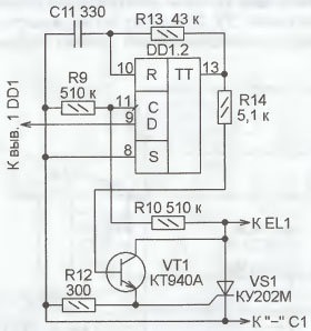
A diagram of another version of the EL1 lamp switching unit is shown in fig. 2. The numbering of elements here continues the one started in Fig. 1. This node is not subject to "hangup", is less critical to the current of the trinistor opening, and most importantly, it turns on the lamp at a lower instantaneous value of the mains voltage. A single vibrator is assembled on the DD1.2 trigger. It starts it in the presence of a permissive high level at the input of the D-flip-flop, the signal supplied to the input C through the voltage divider R9R10. This happens at times when the voltage at the anode of the trinistor rises and reaches about 15 V. While the voltage at input D is logic low, the flip-flop remains low at output 13, transistor VT1 and trinistor VS1 are closed, and the lamp is de-energized. With a high level at input D, the pulses arriving at input C at the beginning of each half-cycle of the mains voltage transfer the trigger to a state with a high level at the output. Transistor VT1 and trinistor VS1 open, voltage is applied to the lamp. Capacitor C11 is charged through resistor R13. After approximately 10 µs, the voltage at the input R of the flip-flop reaches the threshold value and the flip-flop returns to its original state. The trinistor remains open until the end of the half-cycle, and in the next the process is repeated. The features of SCR control units and their application can be found in [3, 4]. SCRs KU202K - KU202R, KU202K1-KU202R1 can be installed in the circuit breaker. If the lamp power does not exceed 400 W, KU201K-KU201N trinistors are also suitable. With a switching power of more than 200 W, the trinistor should be installed on a heat sink. For SCRs of the KU202 series, the opening current of the control electrode is guaranteed to be no more than 100 mA, although in fact for most of them it is several times less. For all specimens tested by the author (about a dozen), this current did not exceed 10 mA. If the DD1 chip in a device assembled according to the circuit shown in Fig. 1, after all, will not be able to give the desired current, a selection of a trinistor may be required. For a node assembled according to the scheme shown in Fig. 2, it is not required to select a trinistor. The KT940A transistor can be replaced with KT940B, as well as with KT604 and KT605 with any letter indexes. All these transistors work quite reliably, although the voltage applied to them formally exceeds the maximum allowable value. Analogue of the diode bridge KBU6G - RS604. Other diode bridges or individual diodes rated for a reverse voltage of at least 400 V and for the current consumed by the lamps controlled by the switch are also suitable. Diodes KD521A will replace any low-power silicon diodes. As an op-amp DA1, not only K154UD1A, but also K154UD1B, as well as 174UD1A, 174UD1B, KR154UD1A, KR154UD1B are suitable. For microcircuits of the 174 and K174 series, a metal case is connected to pin 5. Since the KR174 series microcircuits are made in a plastic case, this pin is left free and it is not required to connect it anywhere. The CZN-15E microphone can be replaced by any other small-sized electret microphone with a built-in FET amplifier. Suitable, for example, the domestic microphone MKE-332. When connecting it, the polarity must be observed. Resistor R1 is selected so that the voltage between the microphone leads is about 5 V. Literature: 1. Micropower operational amplifier 154UD1. - rdalfa.lv/data/oper_usil/1541.pdf.
Author: K. Gavrilov, Novosibirsk; Publication: radioradar.net
Machine for thinning flowers in gardens
02.05.2024 Advanced Infrared Microscope
02.05.2024 Air trap for insects
01.05.2024
▪ The smallest magnifying glass sees bonds between atoms ▪ Electric capsule to stimulate the stomach and improve appetite
▪ section of the site Medicine. Selection of articles ▪ article Let the world perish, but justice be done. Popular expression ▪ article How likely does a photo of a baby in a wallet increase? Detailed answer ▪ article Head of labor protection department. Job description ▪ article A coin jumps out of a glass. Focus Secret
Home page | Library | Articles | Website map | Site Reviews
www.diagram.com.ua |


 Leave your comment on this article: