|
|


 Arabic
 Bengali
 Chinese
 English
 French
 German
 Hebrew
 Hindi
Hindi Italian
 Japanese
 Korean
 Malay
Malay Polish
 Portuguese
 Spanish
 Turkish
 Ukrainian
 Vietnamese
|
ENCYCLOPEDIA OF RADIO ELECTRONICS AND ELECTRICAL ENGINEERING Output power indicator. Encyclopedia of radio electronics and electrical engineering
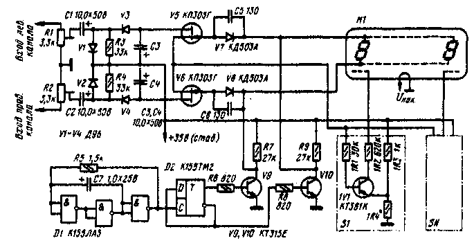
Encyclopedia of radio electronics and electrical engineering / Transistor power amplifiers In indicators of the output power of audio frequency amplifiers, radio amateurs usually use pointer devices and LEDs. However, multi-digit vacuum luminescent indicators IV-18, IV-21, IV-27, IV-28, etc., can be used with no less success in such devices, and one such device is enough to indicate the output power of both channels of a stereo amplifier. This is possible if the upper segments of the signs are used to indicate the power of one of the channels, and the lower segments of the other. In the device offered to the attention of readers, any of the above luminescent indicators can be used. The minimum power recorded by it is 1 W, the dynamic range is about 17 dB. The number of recorded power levels depends on the type of indicator: when using IV-18 indicators. IV-21 it is equal to 8, and indicators IV-28D and NV-27 - respectively 9 and 14. The schematic diagram of the device is shown in the figure. It consists of input voltage dividers for the signals of the left (R1) and right (R2) channels, two rectifiers (V1, V3 and V2, V4), a switch (V5, V6), a clock generator (D1, D2, V9, V10), a set (according to the number of recorded power values) of electronic keys S1-SN and an indicator HI. Controlled signals from the outputs of the rectifiers are fed to the switch, which alternately, with a frequency of about 40 Hz (so that the flickering of the indicator segments is not noticeable), supplies them to the inputs of the electronic switches S1-SN. The switching frequency is set by a clock pulse generator, consisting of the actual generator on the inverters of the D1 microcircuit, the D2 trigger operating in the frequency division by 2 mode, and the switches on transistors V9, V10. The introduction of trigger D2 is due to the need to obtain anti-phase pulses with a duty cycle equal to 2 (otherwise, the brightness of the glow of the segments in the channels would not be the same). Pulses from the trigger output alternately open transistors V9, V10, and the indicator segments connected to the collector of the currently open transistor are connected to a common wire. At the same time, the supply voltage is applied to the segments connected to the collector of a closed transistor, and those of them. which are located under the grids connected to the open transistors of the keys S1-SN, begin to glow.
Each of the keys (the figure shows the diagram of the first of these devices - S1) is triggered at a certain signal voltage at the base of its transistor. The response threshold depends on the voltage at the emitter, which is set by a voltage divider consisting of resistors 1R3, 1R4 in the first key, resistors 2R3, 2R4, etc. in the second key. When the signal voltage at the switch output exceeds the emitter potential by about 0,6 .1 V. The transistor 1V1 is served and the voltage from the dividers 31R4R1 through its section emitter collector and resistor 2R1 is supplied to the first grid of the indicator H2. As a result, the segment located under it from the row to which the supply voltage is applied begins to glow. At the next moment, the supply voltage is supplied to the segments of another row, and if the signal in another channel of the amplifier has the same or higher level, then the first segment of this row also starts to glow. As the signal levels in the channels increase, the keys S3, SXNUMX, etc. are triggered, and two lines of luminous segments are observed on the indicator. At a given supply voltage Upit and the resistance of resistors 1R3 - NR3 equal to 1 kOhm, the resistance of resistors 1R4 - NR4 (in kiloohms) is calculated by the formula
where the response voltage Uср = = VP (Р is the output power in watts). It is not recommended to choose the voltage Ucp greater than 8 V (for the SN key), because otherwise the brightness of the glow of the first and last segments in the lines will be noticeably different. In practice, it is advisable to limit the voltage values Ucp to the limits of 1 and 7,1 V, which corresponds to the recorded power from 1 to 50 W. Details. Almost any small-sized resistors and capacitors can be used in the indicator. D9B diodes can be replaced by any other from the D2 and D9 series, KP303G transistors by others from this series. It is permissible to replace the KT315E and KT361K transistors with any low-power silicon transistors of the appropriate structure with a permissible voltage between the emitter and collector of at least 35 V and a static current transfer coefficient h21e of at least 100. The adjustment of the device begins with a half-boron of resistors 1R4-NR4, ensuring that the voltages at the emitters of transistors 1V1-NV1 (relative to the positive output of the power source) become equal to the calculated values Ucp-0,6. Then, a signal with a frequency of 1000 Hz and a voltage corresponding to the maximum recorded power is applied to the input of the left channel of the indicator (for an output power of 50 W at a load with a resistance of 4 ohms - approximately 14.7 V) and with a tuning resistor R1, all segments of the corresponding row on the indicator H1 are lit. The right channel is calibrated in the same way. To increase the contrast of the image of the luminous rulers, it is necessary to install a green light filter in front of the indicator. Author: S. Fedorov, Malaya Vishera, Novgorod region; Publication: N. Bolshakov, rf.atnn.ru
Machine for thinning flowers in gardens
02.05.2024 Advanced Infrared Microscope
02.05.2024 Air trap for insects
01.05.2024
▪ By 2030, one in five cars in Japan will be self-driving ▪ Compact 3-phase power supply TDR-480 ▪ Ultrasonic tweezers move living cells
▪ section of the website Residual current devices. Selection of articles ▪ article Digital satellite television. History of invention and production ▪ article Who Invented Playing Cards? Detailed answer ▪ article Functional composition of Loewe TVs. Directory ▪ article Cell phone radiation detector. Encyclopedia of radio electronics and electrical engineering
Home page | Library | Articles | Website map | Site Reviews
www.diagram.com.ua |


 Leave your comment on this article: