|
|


 Arabic
 Bengali
 Chinese
 English
 French
 German
 Hebrew
 Hindi
Hindi Italian
 Japanese
 Korean
 Malay
Malay Polish
 Portuguese
 Spanish
 Turkish
 Ukrainian
 Vietnamese
|
ENCYCLOPEDIA OF RADIO ELECTRONICS AND ELECTRICAL ENGINEERING Devices for holding long time intervals. Encyclopedia of radio electronics and electrical engineering
Encyclopedia of radio electronics and electrical engineering / Clocks, timers, relays, load switches The author brings to the attention of readers several simple time delay devices from available parts. These devices are analog with timing RC circuits. They use circuit solutions that make it possible to increase the duration of the generated time intervals. On fig. 1 shows a diagram of a simple time relay assembled on a TL431ACLP (DA1) parallel voltage regulator chip. When the SB1 button is pressed, a voltage close to the supply voltage is supplied to the control input of the stabilizer DA1 through resistors R1 and R3, as a result of which the stabilizer closes the circuit of the relay winding K1. Contacts K1.1 work The fading relay blocks the button, which can now be released. They also disconnect the resistor R1 from the time-setting capacitor C1, which begins to be charged by the current flowing through the time-setting resistor R2. Relay contacts K1.2 turn the actuator on or off. As the capacitor charges, the voltage at the control input of the DA1 chip relative to its anode decreases. As soon as it drops below 2,5 V, the current through the relay winding K1 will decrease so much that the relay will release the armature, returning the actuator to its original state. Resistor R1 will again be connected in parallel with capacitor C1 and will discharge it. Now you can press the SB1 button again. With elements, types and ratings of which are indicated in fig. 1, an exposure of about 45 minutes was obtained. It can be changed by selecting capacitor C1 and resistor R2. But it is not recommended to increase the resistance of this resistor, since this increases the share of the unstable current of the control input of the DA1 microcircuit in the charging current of the capacitor C1. Accordingly, the exposure instability increases.
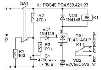
You can increase the resistance of the resistor R2, while simultaneously increasing the supply voltage of the device up to 30 V - the maximum for the TL431 series microcircuit. In this case, the capacitor C1 should also be selected with a rated voltage not less than the supply voltage. As K1, you need to use a relay with an operating voltage of the winding equal to the supply voltage, or connect in series with the relay winding, designed for a lower voltage, quenching excess voltage, a zener diode. The current of the relay winding should not exceed 100 mA, allowed for the TL431 series microcircuit. On fig. 2 shows another circuit of the delay relay for turning on or off the actuator, built on the same microcircuit. After switching the switch SA1 to the "On" position (the upper group of its contacts according to the diagram is closed, and the lower one is open), the charging of the capacitor C1 through the resistor R2 begins. When the voltage across the capacitor exceeds the sum of the stabilization voltage of the zener diode VD2 (5,6 V), the threshold voltage of the stabilizer DA1 (2,5 V) and the voltage drop across the resistor R3 and the diode VD1, the DA1 chip will close the circuit of the relay winding K1. A triggered relay will change the state of the actuator. The device will remain in this state until switch SA1 is returned to its original off state. When shown in Fig. For 2 types and ratings of elements, an exposure of about one hour was obtained.
As threshold elements in such devices, you can use not a TL431 series microcircuit, but an insulated gate field effect transistor. Such transistors are known to have an extremely low gate current. This allows you to significantly increase the shutter speed by using time-setting resistors with a resistance of up to several megaohms and even tens of them. In addition, the use of, for example, a 2N7000 field-effect transistor allows you to increase the supply voltage to 60 V and, if necessary, use an electromagnetic relay with a winding current of up to 250 mA. But measures should be taken so that the voltage between the gate and the source of the transistor does not go out of the permissible range from -20 V to +20 V. An example of a turn-on delay relay circuit based on a 2N7000 field-effect transistor is shown in fig. 3. Relay K1 - imported BT series with a winding resistance of 62,5 ohms. With the ratings of the elements indicated in the diagram, an exposure of about six hours was obtained. For most of the exposure interval, the device practically does not consume current from the power source. But in the last third of this interval, the current gradually increases to the current of relay K1 operation. In this period of time, the transistor VT1 is in active mode and a rather significant power is dissipated on it, reaching a maximum (in this case, about 150 mW) approximately in the middle of the gap, and then falling off.
After relay K1 is activated, the current continues to rise to a value equal to the difference between the supply voltage of the device and the stabilization voltage of the zener diode, divided by the resistance of the relay winding. Having reached it, it remains so until the time relay is turned off by switch SA1. In the device, the scheme of which is shown in Fig. 4, the same idea is used as in the previous one, but to reduce the current consumed after operation, a polarized relay with two stable states RPS20 version RS4.521.751 is used. It has two groups of contacts for switching.
After pressing the SB1 button, the voltage supplied through the resistor R1 and the voltage divider R2R3 to the gate of the field-effect transistor VT1 opens this transistor. The voltage applied to the left winding of the relay K1 according to the diagram, transfers its moving contacts to the lower position according to the diagram, which blocks the SB1 button and allows the charging of capacitors C1 and C2. After some time required to charge the capacitor C1, the transistor VT1 will be closed, and the current through the left winding of the relay will stop, which will not change the state of its contacts. After the capacitor C2 is charged and the drain current of the transistor VT2 reaches a value sufficient to transfer the right winding of the relay of its contacts to its original (upper according to the diagram) position, discharge resistors R1 and R5 will be connected to the time-setting capacitors, and the power from the device will be turned off. Now it does not consume current, and after discharging the capacitors, it is ready for the next press of the SB1 button. Obviously, the maximum time delay of devices assembled according to the schemes shown in Fig. 3 and fig. 4 is the same. Resistors R2 and R3 in the latter are chosen such that the gate-source voltage of the transistor VT1 does not exceed the permissible value. Since a long exposure time from the node on this transistor is not required, it can also be bipolar. In this case, the resistors R2 and R3 must ensure that the transistor VT1 is in saturation mode from the charging current of the capacitor C1. On fig. 5 shows a diagram of a long-duration pulse generator, which can be used to periodically turn on and off any devices. In essence, these are two devices according to the previously discussed scheme in Fig. 3, which, thanks to the use of a polarized bistable relay, form a kind of multivibrator. The duration of each of the two repeating time intervals can be set independently by selecting the elements of the R2C1 and R3C2 circuits.
It should be noted that all the described devices should be powered with a stabilized voltage to obtain a stable shutter speed. Installing in them oxide capacitors of equal ratings, but produced at different times by different manufacturers, gives a significant spread in exposure values. Leakage currents of time-setting capacitors and changes in ambient temperature significantly affect the exposure. Therefore, all the values of the timing elements indicated on the diagrams are approximate. They will have to be selected when setting up the device. In order not to wait hours for their operation when checking the operation of the described devices, it is recommended to temporarily replace the time-setting resistors in them with others having a resistance 100 ... 1000 times less than that indicated on the diagram or calculated. Only after making sure that the device is working and measuring the shutter speed given to it, replace the temporary resistors with constant ones, increasing their resistance as many times as the required shutter speed is greater than the measured one. But keep in mind that with a large resistance of the timing resistor, the proportionality of exposure to its resistance may be violated. The reason for this is the influence of the capacitor leakage current and the input current of the microcircuit or bipolar transistor. In order not to miss the moment of the end of the exposure, during the adjustment process it is convenient to connect a piezo sound emitter with a built-in generator to the output of the time relay. In this case, before his signal, you can safely do other things. Author: M. Muratov
Machine for thinning flowers in gardens
02.05.2024 Advanced Infrared Microscope
02.05.2024 Air trap for insects
01.05.2024
▪ pig city ▪ Chinese electric bus BYD - 325 km on a single charge
▪ section of the site Fundamentals of safe life (OBZhD). Article selection ▪ article I'm someone no one likes. Popular expression ▪ article Why did the ace of cards go from one to the highest card? Detailed answer ▪ headband article. Health care ▪ article Digital tone block. Encyclopedia of radio electronics and electrical engineering
Home page | Library | Articles | Website map | Site Reviews
www.diagram.com.ua |


 Leave your comment on this article: