|
|


 Arabic
 Bengali
 Chinese
 English
 French
 German
 Hebrew
 Hindi
Hindi Italian
 Japanese
 Korean
 Malay
Malay Polish
 Portuguese
 Spanish
 Turkish
 Ukrainian
 Vietnamese
|
ENCYCLOPEDIA OF RADIO ELECTRONICS AND ELECTRICAL ENGINEERING Quasi-sensor relay switches. Encyclopedia of radio electronics and electrical engineering
Encyclopedia of radio electronics and electrical engineering / Clocks, timers, relays, load switches In the manufacture of one of the devices, I needed a three-position three-way switch (3P3N). The device is small and light, so one of the main requirements for the switch was the minimum switching force. Mechanical switches (galette, push-button, sliding) did not meet this requirement. I found a way out in the manufacture of a switching unit with the desired switching circuit based on electromagnetic relays and microswitches.
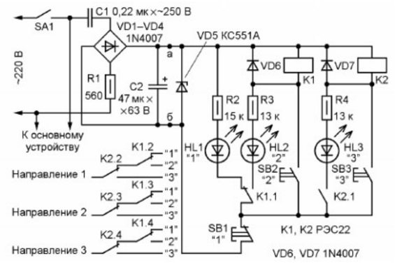
The diagram of the 3P3N relay switch is shown in fig. 1. It is controlled by three buttons (SB1-SB3), and switching is carried out by two relays (K1, K2) with four groups of switching contacts each, one of them is used for self-locking of the relay, and the other three are used for switching circuits of the main device. The switch is powered by a transformerless unit containing a ballast capacitor C1, a rectifier bridge VD1-VD4 and a filter capacitor C2. Resistor R1 limits the inrush current through the bridge diodes at the moment of switching on, the output voltage is limited by the zener diode VD5. When power is supplied by the switch SA1 of the main device, a voltage of approximately 50 V appears at the output of the power supply unit of the switch. A current of about 1.1 mA, limited by resistor R1, flows through the normally closed contacts K2 and the LED HL4. Relays K1 and K2 are de-energized. The HL1 LED is on, indicating the position "1" of the switch. When you press the SB2 button, relay K1 is activated. With contacts K1.1, it is self-locking, i.e. it remains on after the button is released. Through the resistor R3 and the lit LED HL2, a current flows that exceeds the release current of the relay. Contacts K1.2-K1.4 switch to position "2". When the SB3 button is pressed, relay K2 is self-blocking with contacts K2.1 and the HL3 LED lights up, with contacts K2.2-K2.4 the switch is switched to position "3". The transition to position "1" is made by pressing the button SB1, which de-energizes the relay windings K1 and K2. The switching circuit of the switch is shown in the lower left part of fig. 1. There are no special requirements for details. Capacitor C1 - film noise suppression. It can be replaced by two K73-17 capacitors connected in series with a capacity of 0,47 microfarads and a rated voltage of 630 V. Capacitor C2 is oxide K50-35 or imported, resistors are of any type. We will replace the VD5 zener diode with a circuit of several low-power zener diodes connected in series with a total stabilization voltage of 45.50 V. Relays K1 and K2 - RES22 (passport RF4.500.130 or version RF4.523.023-06). Their operating voltage is 48 V, the winding resistance is 2250 ... 2875 Ohm, the actuation and release current are 10,5 and 2,5 mA, respectively. Microswitches MP1-3 are used as buttons SB3 - SB1. LEDs HL1-HL3 - any diameter of 3 mm, preferably high brightness. The switch parts are mounted on the same universal breadboard as the main unit. Pieces of tinned copper wire with a diameter of 0,5.0,6 mm are soldered to the relay outputs. These new pins are inserted into the holes of the breadboard and after the maximum possible approach of the relay to the board, they are soldered to its pads. Several large drops of hot-melt adhesive are introduced into the space between the relay case and the board by means of a pistol. After it cooled, a rigid and mechanically strong structure was obtained. This method of mounting the relay made it possible to avoid the manufacture of a bracket for its fastening and the use of a bundle of one and a half dozen wires for its connection.
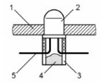
To save space on the front panel, the pushers of the SB1-SB3 buttons are made using HL1-HL3 LEDs. A similar design of the buttons is described in O. Shaida's note "Button made of LED" ("Radio", 1995, No. 9, p. 45). The sleeves used by the author could not be found, therefore, instead of them, segments of a written rod with a diameter of 4,5 mm from a gel fountain pen were used. At one end of the segments 3 (Fig. 2), diametrical cuts 3 mm deep were made, on the other side, the leads of the LED 2 were inserted inside until the LED housing abutted against the end of the segment. The leads 5 of the LED are brought out through the slots, and the segment is plugged with a drop of hot-melt adhesive 4. After it hardens, the end is trimmed with a scalpel. Finally, the LEDs are inserted into the holes provided for this in the device control panel 1, and their outputs are connected by segments of a flexible mounting wire MGTF 0,07 to the corresponding contact pads of the board. Such a design is very convenient - the button that glows after pressing indicates the position of the switch. If the LED housing is made of colorless plastic, then to increase the LED emission angle, it must be made matte by processing it with fine-grained (“micron”) sandpaper. The switch, as practice has shown, turned out to be successful - ergonomic, reliable and easy to install, so I widely used it in my designs. In the manufacture of one of the subsequent devices, a power reserve was revealed in the power supply, so it was decided to make a switch with a digital indication of the on position.
The diagram of this switch option is shown in fig. 3. It works like this. After the power is turned on, relays K1 and K2 remain off, since the current through their windings, determined by the resistance of resistors R2 and R9, is approximately 3 mA, which is less than the pick-up current, but more than the release current. This is the position "1" of the switch, as evidenced by the number 1 displayed on the HG1 indicator (voltage is supplied to its elements "b" and "c" through current-limiting resistors R3, R4). When you press the SB2 button, its contacts close the resistor R2, the current through the relay winding K1 increases, and it works. After the button is released, the relay remains on because the current through the coil exceeds the release current. The switched contacts K1.1 remove the voltage from the element "c" and apply it to the elements "e" and (through the VD7 diode) "a", "d", "g", so the HG1 indicator lights up the number 2. Similarly, when you press the button SB3 is activated and remains in the on state of relay K2, switching the switch to position "3", in which voltage is supplied to the corresponding elements of the indicator through contacts K2.1 and diodes VD6, VD8. The switch is returned to its original position "1" by breaking the power supply circuit of the relays K1 and K2 with the SB1 button. The switching circuit of this switch is the same as the switch according to the diagram in Fig. 1. To control the switch, small-sized buttons dismantled from old office equipment were used. When re-manufacturing this device, I encountered a difficulty - there was no button with an opening (normally closed) contact at hand, while there were plenty of membrane buttons with a closing (normally open) contact from old video equipment. Under these buttons, the circuit has been changed, as shown in Fig. 4 (switching circuit remained the same).
In this switch, when the power is turned on, the current flowing through the zener diode VD5 opens the transistor VT1, but both relays, as in the previous version, remain off, since the current flowing through their windings only slightly exceeds the release current. The switch is moved to position "2" by pressing the button SB2, to position "3" - by pressing the button SB3. To move to position "1" button SB1 close the emitter junction of the transistor VT1. In this case, the transistor closes and the relays return to their original state "1". To indicate the switch positions, you can use both a digital indicator and individual LEDs by turning them on in series with current-limiting resistors in the relay winding circuits, as shown in fig. 1. When choosing a replacement for the KT815G transistor, it must be taken into account that for reliable operation of the switch, the allowable voltage U^ of the transistor must be at least 80 V.
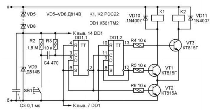
In some cases, for example, with remote control of switching, it is desirable to use one button, sequentially (along the ring) passing through all positions. A diagram of such a switch is shown in fig. 5. Resistors R2, R3 and capacitor C4 are used to suppress the "bounce" of the contacts of the button SB1, which works as follows. When the power is turned on, a voltage of about 9 V appears on the Zener diode VD9, which is used to power the DD1 chip. Capacitor C4 remains discharged. When you press the SB1 button at the moment of the first touch of the button contacts, the capacitor C4 is instantly charged through the resistor R3. Further bounce of the button contacts does not affect the output voltage, since the capacitor C4 is discharged through the resistor R2 of much higher resistance. Trigger DD1.1 switches at the moment of voltage drop at the synchronization input (pin 3). Transistor VT2 switches twice as often as transistors VT1 and VT3. When the SB1 button is pressed, the switching node goes through all possible states in turn: the relays are de-energized, the relay K1 is activated, the relay K2 is activated, the relays are de-energized, etc. The device status is displayed by a digital indicator, switched on in accordance with the diagram in fig. 2. As in the previous version of the switch, the allowable voltage U^ of transistors VT1 and VT3 must be at least 80 V.
If necessary, using another relay and an additional button, you can assemble a switch for four positions and three directions (Fig. 6), which can be used, for example, for switching ranges in a generator or frequency meter. It is also possible to enter a digital indication of the position into it by making appropriate changes to the circuit for including the indicator elements. PS The 3P3N switches described in the article have a drawback, which is that after being set to position "3", in which both relays are on, they can only be switched to position "1" (return to position "2" is impossible). Similarly, after setting the 4P3N switch to position "4", when all three relays are on, it is possible to return to position "2" or "3" only after having previously "been" in position "1". The RES22 relays used by the author (passport RF4.500.130) are replaceable relays of this type of execution RF4.523.023-02, however, they have a higher release current (3,5 instead of 2,5 mA), so the resistance of the resistors connected in series with their windings must be reduced from 13 up to 9,1 kOhm Author: K. Moroz
Machine for thinning flowers in gardens
02.05.2024 Advanced Infrared Microscope
02.05.2024 Air trap for insects
01.05.2024
▪ Brain implant for memory recovery ▪ Quick measurement of magnetic field parameters ▪ Ultrabook Toshiba dynabook V632 has 13 hours battery life ▪ Artificial intelligence will distinguish the original painting from a fake ▪ Tidal floods are associated with a special type of slow ocean wave.
▪ site section Power supplies. Article selection ▪ article Andrei Kolmogorov. Biography of a scientist ▪ article Who are bards? Detailed answer ▪ article Bed bayonet. Travel Tips ▪ article Spot welding on chokes. Encyclopedia of radio electronics and electrical engineering ▪ article Three phases - from one. Encyclopedia of radio electronics and electrical engineering
Home page | Library | Articles | Website map | Site Reviews
www.diagram.com.ua |


 Leave your comment on this article: