|
|


 Arabic
 Bengali
 Chinese
 English
 French
 German
 Hebrew
 Hindi
Hindi Italian
 Japanese
 Korean
 Malay
Malay Polish
 Portuguese
 Spanish
 Turkish
 Ukrainian
 Vietnamese
|
ENCYCLOPEDIA OF RADIO ELECTRONICS AND ELECTRICAL ENGINEERING Theory: AF power amplifiers. Encyclopedia of radio electronics and electrical engineering
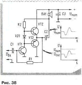
Encyclopedia of radio electronics and electrical engineering / Beginner radio amateur To combat distortion of the "step" type, a small initial bias voltage is applied to the bases of the transistors of the UMZCH output stage, setting the class B mode or. to ensure that there is no distortion, class AB, by passing a small initial current through the transistors - the quiescent current. Another way is to introduce negative feedback (NFB). reducing distortion. Often both options are used together. Because the voltage divider designed to create the initial bias draws some current. it is convenient to use the current of the terminal stage, which amplifies the voltage and operates in class A mode. The UMZCH circuit with a pre-terminal amplifying stage and a unipolar power supply is shown in fig. 38.
Let's take a closer look at his work. The input signal through the decoupling capacitor C1 is fed to the base of the transistor VT1 of the final stage. The bias is supplied through the resistor R1. In fact, as we saw earlier, this resistor should be connected between the base and collector of transistor VT1. However, given that the output stage is an emitter follower, it is still better to connect it to the output, where the DC voltage is the same, but the OOS will also cover the output stage, reducing signal distortion. The VD1 diode is connected in the forward direction to the collector circuit of the transistor of the preamp stage, the voltage drop across which creates the initial bias at the bases of the output stage transistors. It would be possible to include a resistor with a small resistance instead of a diode, but the diode provides better temperature stability for the entire amplifier. The fact is that with increasing temperature, the base-emitter voltage of the output transistors decreases, which is necessary to provide the selected quiescent current. The forward voltage across the diode also decreases with increasing temperature, which prevents the quiescent current from increasing. For powerful amplifiers, this diode is placed on the radiator of the output transistors. To adjust the quiescent current, select the number of diodes connected instead of VD1 in series or in parallel. You can add a tuning resistor to the diodes. The signal amplified by the current output stage is fed through a high-capacity isolation capacitor C2 to the dynamic head BA1. Capacitor C3, also large, shunts the power supply. It is needed when the battery is partially discharged and its internal resistance has increased. Then the capacitor, accumulating the energy of the battery, ensures the return of large current pulses to the load at loudness peaks. With mains power, it can be a smoothing capacitor of the rectifier. Pay attention to the connection of the load resistor of the pre-terminal stage - not to the plus of the power source, but to the output of the dynamic head BA1. This does not affect the DC amplifier mode, since the head resistance is small, but the amplifier's operation at audio frequencies is noticeably improved as a result of the resulting "voltage boost". When a positive half-wave of the signal acts at the input of the amplifier, the current of the transistor VT1 increases, and the voltage at its collector drops, forming a negative half-wave of the output signal. In this case, part of the collector current branches into the base-emitter junction of the transistor VT3, opening it. When a negative half-wave of the input signal acts at the input of the amplifier, transistors VT1 and VT3 close, and VT2 opens with a current flowing through the load resistor R2. If its resistance is significant, transistor VT2 opens worse than VT3. which leads to the limitation of the positive half-waves of the output signal, i.e. to distortion. By connecting the resistor R2 to the bottom output of the dynamic head according to the circuit, we largely eliminate these distortions, since the instantaneous voltage at this output with a positive half-wave of the output signal becomes greater than the supply voltage. This provides the best "buildup" of the transistor VT2. In conclusion, we give an approximate calculation of this amplifier. Let's say that the supply voltage is 6 V and the resistance of the dynamic head is 6 ohms (you can use other data). It can be seen from the oscillograms that the amplitude of the output signal cannot exceed half the supply voltage, i.e. 3 V. The maximum amplitude of the current in the head will therefore be 3 V / 6 Ohm = 0.5 A. The maximum output power of the amplifier is equal to half the product of the amplitude values of current and voltage and will be 0.75 W. The average current consumed from the power supply in the case of class B mode setting is 0,32 peak value, i.e. 175 mA, and power consumption - 1.05 W. In class AB mode and current. and more power consumption. From this it is clear that medium power transistors must be used in the output stage. The calculation of the preterminal cascade is even simpler. If we ask ourselves the static current transfer coefficient of the output transistors (say 50). then we can determine the amplitude of the alternating current in their bases. It will be 0.5 A / 50 = 10 mA. The collector current of the preterminal stage should also be the same. Since half the supply voltage drops across the load resistor R2, we determine its resistance: 3 V / 0,01 A \u300d XNUMX Ohms. We find the resistance of the resistor R1 by multiplying the load resistance by the static current transfer coefficient of the transistor VT1. If it is equal to, for example, 100, then the resistance will be 30 kOhm. This resistor is easier to choose experimentally by measuring the voltage at the emitters of the output transistors - it should be half the voltage of the power source. From such an approximate calculation, it is clear that in order to increase the efficiency and effectiveness of the UMZCH, it is advantageous to use transistors with a high value of the current transfer coefficient. Author: V.Polyakov, Moscow
Traffic noise delays the growth of chicks
06.05.2024 Wireless speaker Samsung Music Frame HW-LS60D
06.05.2024 A New Way to Control and Manipulate Optical Signals
05.05.2024
▪ Intel Clover Falls Auxiliary Chip ▪ Space station in a giant asteroid ▪ In the heat is not up to love
▪ website section LEDs. Article selection ▪ article Upper Volta with ballistic missiles. Popular expression ▪ article How do we know what is at the center of the Earth? Detailed answer ▪ article Content manager (website editor). Job description ▪ article Lighting off delay machine. Encyclopedia of radio electronics and electrical engineering
Home page | Library | Articles | Website map | Site Reviews
www.diagram.com.ua |

 Leave your comment on this article: