|
|


 Arabic
 Bengali
 Chinese
 English
 French
 German
 Hebrew
 Hindi
Hindi Italian
 Japanese
 Korean
 Malay
Malay Polish
 Portuguese
 Spanish
 Turkish
 Ukrainian
 Vietnamese
|
ENCYCLOPEDIA OF RADIO ELECTRONICS AND ELECTRICAL ENGINEERING Adjustable charging current stabilizer. Encyclopedia of radio electronics and electrical engineering
Encyclopedia of radio electronics and electrical engineering / Automobile. Batteries, chargers A powerful transistor is often used as a regulating element of a charger. This transistor, which operates in a linear mode, dissipates a lot of thermal power, which is why it has to be installed on a bulky heat sink. The efficiency of such devices is usually low. I propose a device in which a pulsed method of regulating the charging current is used, and a trinistor as a regulating element, which can significantly reduce energy losses. Main Specifications Maximum charging current, A ..... 6
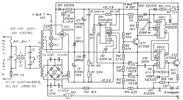
Schematic diagram of the current stabilizer is shown in fig. 1. The device consists of a network noise suppression filter formed by a two-winding choke L1 and capacitors C1-C3, a network transformer T1, a powerful rectifier based on diodes VD3-VD6, a low-power rectifier VD2 with a bipolar parametric stabilizer VD7R2VD8R3, a current setting unit - a variable resistor R4, a current sensor R14 with a two-link RC filter R12C14R11C13, an error signal amplifier at the op-amp DA1, a voltage sensor on the transistor VT1, necessary to determine the moments when the mains voltage passes through zero, an adjustable single vibrator on the DD1.1 trigger and a single vibrator on the DD1.2 trigger with current amplifier on the transistor VT2, which generate control pulses of the trinistor VS1, which ultimately regulates the charging current. From the engine of the variable resistor R4 through the resistor R6, a negative voltage is supplied to the inverting input of the op-amp. The parameters of the circuit of the resistive divider R4R5 are calculated in such a way that it is more negative than at the non-inverting input of the op-amp, therefore, a positive signal is formed at the output of the op-amp, proportional to the difference in the input voltage values. This signal, through the resistor R13, enters the time-setting circuit of a controlled single vibrator assembled on a D-trigger DD1.1 [1]. A feature of this one-shot is a proportional decrease in the duration of the pulse generated by the one-shot with an increase in the input signal level. The beginning of the single vibrator pulse is "tied" to the beginning of the half-cycle of the mains voltage using a voltage sensor made on the transistor VT1. A pulsating voltage is supplied to the base of this transistor through resistor R8 from the rectifier bridge VD2. Diode VD1 "decouples" this circuit from the smoothing capacitor C8. The resistance of the divider resistors in the base circuit of the transistor is calculated in such a way that most of the time the transistor is open, and only at the moments when the output voltage of the bridge drops to almost zero, the transistor closes and a short positive pulse from its collector is transmitted to the input S of the trigger DD1.1. The trigger switches to a single state, the capacitor C15 begins to charge, and when the voltage on it, and hence at the input R of the trigger, reaches the switching threshold, the trigger will return to the zero state. The charging current of this capacitor has two components: through the R17R16VD10 circuit from a stable voltage source (+12,5 V) and the R13VD9 circuit from a variable voltage source (from the output of the op-amp). The greater the output voltage of the op-amp, the greater the second component of the charging current, the faster the capacitor charges and the shorter the high-level pulse at the direct output of the trigger. Thus, depending on the pulse duration of the controlled single vibrator, the trinistor will turn on with a different delay from the beginning of the half-cycle. Accordingly, the current coming from the powerful rectifier will also change. That is, the position of the slider of the resistor R4 sets the average value of the charging current. The OS voltage, taken from the resistor R14 and proportional to the load current, after smoothing with a two-link filter R12C14 R11C13, is applied in negative polarity to the non-inverting input of the op-amp. If the charging current decreases, for example, due to an increase in the EMF of the battery being charged, the voltage at the non-inverting input will become less negative, the output voltage of the op-amp will increase, which will lead to a decrease in the pulse duration of the adjustable single vibrator, and hence to a decrease in the turn-on delay of the trinistor VS1 - the current will increase. The gain of the op-amp is equal to the ratio of the resistance values of the resistors R7 and R6: 1 MΩ: 2 kΩ = 500 Therefore, the stabilizer responds to the smallest changes in current. Lamps HL1, HL2 illuminate the scale of the PA1 ammeter and at the same time serve as an indicator of the device being turned on. Resistor R1 is selected so that the voltage on the lamps is 5 ... 6% lower than the nominal. Capacitors C4-C7, shunting diodes of a powerful rectifier, reduce the level of high-frequency interference penetrating the network. Capacitor C12 eliminates the self-excitation of the op-amp (it is installed if necessary). OU K140UD1B can be replaced by K140UD6, K140UD7, and the KD510A diode - by KD509A, KD513A. In a powerful rectifier, diodes KD2999A, KD2999B, as well as D242, D243 (with an increase in the effective area of heat sinks) can be used. Zener diodes D814D are interchangeable with D814G. Instead of the trinistor KU202N, KU202L, KU202I are suitable. Capacitors C1-C7 - K73-16, K78-2; C8-SU, C13, C14 - K50-35; C11, C12, C15, C16 - KLS, KM-6. Resistor R4 - PPZ-12, a R5, R17 - SP5-ZV; R14 - 2 resistors C5-16MV with a resistance of 0,1 ohms, connected in parallel (each of them can be replaced with a length of 72 mm of nichrome wire with a diameter of 1 mm). Lamps HL1, HL2 -CMH10-55 (CMH10-55-2). Ammeter RA1 - M4205 with an external shunt for 10 A. The inductor L1 is wound on an annular magnetic circuit of size K20x10x5 made of 2000NM ferrite with a MGTF 0,5 wire folded in half, the number of turns is 24. The resulting two windings are switched on as shown in the diagram. Transformer T1 is made on a steel magnetic circuit ShL25x40, winding I contains 1012 turns of wire PEV-2 0,5; winding II - 144 turns of wire PEV-2 0,2 with a tap from the middle; winding III - 104 turns of wire PEV-2 1,6. Diodes VD3-VD6 are installed on four copper plates-heat sinks with an area of 60 cm2 each. The heat sink of the trinistor VS1 has an area of 100 cm2.
Most of the parts of the device are mounted on a printed circuit board made of fiberglass laminated on one side with a thickness of 1,5 mm. On fig. 2 shows a drawing of a printed circuit board and the location of parts on it. Two holes, near the middle of the board, are designed to fix the trimming resistors R5 and R17. The cases of these resistors are installed on the board, close to each other, with adjusting screws towards the edge of the board and attracted with a bar and screws with nuts. Setting up the device should begin with checking the bipolar supply voltage of the OS. If necessary, select zener diodes and their ballast resistors. Next, using an oscilloscope, they check for the presence of short high-level pulses with a period of 1 ms at the collector output of transistor VT10. It is desirable to achieve the minimum duration of these pulses by selecting the resistor R8. An oscilloscope is also needed to check the duration of low-level pulses at the inverse output of an adjustable single vibrator DD1.1 (pin 2). This is done with the charging current stabilization system turned off, for which it is enough to temporarily connect the non-inverting input of the op-amp to the common wire. The engine of the tuning resistor R5 is set in such a position that the change in the pulse duration at the inverse output of the trigger DD1.1 from 0 to 10 ms corresponds to a full rotation of the shaft of the variable resistor R4. In this case, it may be necessary to adjust the position of the shaft of the resistor R17. It should be noted in conclusion that those who undertake the manufacture of the device described above, it will be useful to familiarize themselves with the publications [3; four]. Literature: 1. Samoylenko A. Controlled single vibrator. - Radio, 1999, No. 5, p. 38, 39. Author: V. Klimov, Moscow; Publication: radioradar.net
Artificial leather for touch emulation
15.04.2024 Petgugu Global cat litter
15.04.2024 The attractiveness of caring men
14.04.2024
▪ Pacemaker working from the heart ▪ In Africa, too, they can build a synchrotron ▪ Curcumin Prevents Vision Loss
▪ section of the website Residual current devices. Selection of articles ▪ article Illusions of depth perception. Encyclopedia of visual illusions ▪ article Why will we never forget Caesar? Detailed answer ▪ article Burns. Types of burns. Burn prevention. Health care ▪ article Four magic rings. Focus secret
Home page | Library | Articles | Website map | Site Reviews
www.diagram.com.ua |


 Leave your comment on this article: