|
|


 Arabic
 Bengali
 Chinese
 English
 French
 German
 Hebrew
 Hindi
Hindi Italian
 Japanese
 Korean
 Malay
Malay Polish
 Portuguese
 Spanish
 Turkish
 Ukrainian
 Vietnamese
|
ENCYCLOPEDIA OF RADIO ELECTRONICS AND ELECTRICAL ENGINEERING Transistor transmitter for the 432 MHz band. Encyclopedia of radio electronics and electrical engineering
Encyclopedia of radio electronics and electrical engineering / Transmitters The description of this transmitter was published in RADIO REF magazine by F8CV. The output power of the transmitter is relatively small, about 100 mW, but this is quite enough to make communications over short distances or, by "fastening", for example, a hybrid amplifier manufactured by Motorola or RCA, to get a "full-fledged" transmitter with an output power of several tens of watts. The transmitter diagram is shown in Fig.1.
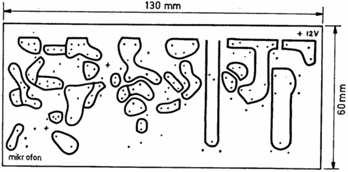
Transistor T2 operates in a crystal oscillator circuit at a frequency of 72 MHz. A modulation amplifier is assembled on transistor T1, a signal from a microphone is fed to the base T1. The amplified signal, through an isolation capacitor, is fed to a varicap connected in series with the L1 coil and a quartz resonator. The modulating voltage changes the capacitance of the varicap and, accordingly, the frequency of the crystal oscillator, thus providing FM modulation. The amplification of the microphone UZCH is set by the potentiometer P, with a resistance of 10 kOhm, by changing the supply voltage of the amplifier. The crystal oscillator circuit is classic and, usually, with serviceable parts and proper installation, it immediately starts working. The quartz oscillator is followed by a frequency tripler on the transistor T3, in the collector circuit of which a circuit is installed, tuned to a frequency of 216 MHz. A distinctive feature of the tripler is the increased input impedance of the cascade, the use of inductive-capacitive coupling with the generator [you can make C8 trimmer, which will increase the voltage filtering of the quartz oscillator, better match the cascades to each other and thereby increase the output power of the transmitter as a whole, because , the coupling coil with the capacitor form a series oscillatory circuit (you may have to select the number of turns of the coupling coil and better match it with the tripler)]. In the T3 emitter circuit, a serial oscillating circuit L4C9 is included, connected in parallel with the resistor R15 and tuned to triple the frequency of the quartz oscillator - 216 MHz, it is provided (with just one circuit!) To almost zero suppression of the frequency of the generator and its harmonics (especially, the second - 144 MHz and the fourth - 288 MHz, except, of course, useful, the third) due to the frequency-dependent negative feedback on the RF current. Thus, at the output of the tripler there is a fairly clean output signal with a frequency of 216 MHz. The next cascade on transistors T4 and T5 - a frequency doubler from 216 MHz to 432 MHz, is made according to a push-pull circuit, moreover, the outputs of the transistor collectors are connected together [such circuits emit even harmonics and suppress odd ones if you turn on this cascade in the usual way with loads in the collector circuits, then odd harmonics will stand out, including the first (amplifier), and even ones, on the contrary, will be suppressed]. At the output of this stage, there is already a fairly high level of output power, sufficient to build up the final stage. It is important to ensure the complete symmetry of the doubler stage [both hardware and signal]. It would be logical to connect the emitter terminals of the frequency doubler transistors T4 and T5 with each other and install one common resistor between them and the case, blocking it in RF with one capacitor, however, in order to ensure better symmetry, it is necessary to make the emitter circuits separate [can also be installed instead of constant resistors R16 and R17 one tuning resistor with a resistance of 160:180 Ohm between the outputs of the emitters, grounding the output of its engine, then it will be possible to smoothly operationally balance the cascade]. The RF power received after the doubler at a frequency of 432 MHz is fed to the L5 strip line, and there are three strip lines in the transmitter: L5, L6 and L7, they are made of printed circuit board foil [it is known that at 432 MHz fiberglass is already starting to "limp", t i.e., losses in the dielectric increase, so it is desirable to "compensate" them at least a little by polishing the line to a mirror finish and covering it from oxidation with a good electrical insulating varnish with low microwave losses, gilding or silvering the line. The best option would be in the case of a polished, silver-coated line placed on a fluoroplast (Teflon) board, with a shortage of foil fluoroplast, a combined board can be used, placing only the final cascade with lines on the "fluoroplast". The cascade on the transistor T6 is the output stage of the transmitter, operates at a frequency of 432 MHz in class AB. The opening bias to the base of the transistor is supplied from the "plus" of the power source through a chain of resistors R18 and R19, a silicon diode is connected between their connection point and the case as a low-voltage zener diode. In the absence of "buildup" in the collector circuit of transistor T6, a quiescent current of 2:3 mA flows. The strip line L6 is the collector load of the terminal power amplifier of the transmitter, the strip line L7 operates in the P-filter circuit to match the output impedance of the transistor with the input impedance of the antenna. Branch to the antenna from 10 mm from the "cold" end of the line. Design and details: to build the transmitter, it is necessary to make a circuit board from foil fiberglass or (even better) from foil fluoroplast (Teflon) with dimensions of 130 x 60 x 1,5 mm. The location of parts on the circuit board is shown in Fig.2. On Fig. Figure 3 shows a sketch of the printed conductors of the circuit board (for convenience, a negative image is shown: foil is indicated in white). Placement of parts on the board, as a rule, does not cause difficulties, since there is enough space on it. Particular attention should be paid to the manufacture of coils. Coil L1 contains 9 turns of winding wire with a diameter of 0,3:0,35 mm on a frame with a diameter of 6 mm. The coil of the L2 crystal oscillator contains 6 turns of the same wire on a frame with a diameter of 4 mm, the coupling coil is wound between the turns of the L2 coil from its "cold" end and has 4 turns of the winding wire of the same diameter as that of L2 (Fig. 4).
The winding of the L3 coil and the paraphase coupling coil should be given increased attention: first, 3 turns of winding wire with a diameter of 5 mm are wound on a mandrel with a diameter of 0,8 mm, then we twist two wires, it is possible to install single-core with multi-colored insulation with a copper diameter of 0,15: 0,2, 3 mm. The winding of the paraphase coupling coil (5 turns) should be made as shown in Fig. 3, at the "cold" end of the coil L6, laying on it, first, two turns of the coupling coil, and, on top of them, the third. Then, the beginning of one wire of the communication coil is connected to the end of the second one (Fig. 4), the wires connected together are soldered to the common wire of the board, the rest - to the bases of transistors T5, TXNUMX. Thus, a tap from the middle and a symmetrical coupling coil are obtained.
Since the frequency of 216 MHz is already quite high, in order to reduce its penetration to the transmitter output due to parasitic mounting capacitances, the terminals of the bases of transistors T4 and T5 are not passed into the holes of the board on the side of the printed tracks, but are connected above the board by surface mounting with short, sufficient for soldering, conclusions. How this is done is shown in Fig. 7, using the example of transistor T5.
All circuits should be mounted with the shortest possible leads, remembering that one centimeter of the length of the wire or lead at a frequency of 216 MHz corresponds to about a meter at frequencies near 2 MHz, you will not mount parts in HF equipment with meter leads! When setting up, you can measure the voltages on each half of the coupling coil with an RF voltmeter with transistors connected and slightly further balance its winding by biting off one of the leads (with a lower voltage) with side cutters. Solders should be protected from oxidation with electrical insulating varnish. Coil L4 is wound with a winding wire with a diameter of 0,45 mm on a mandrel with a diameter of 4 mm and contains 6 turns. The RF choke in the collector circuits of the frequency doubler transistors has 4 turns of wire with a diameter of 0,45 mm on a mandrel of 2,5 mm. The remaining two chokes have 4:5 turns of insulated wire and are wound on small ferrite tubes (Fig. 8). The number of turns is not critical.
The conclusions of the mounted transistors must be of the minimum length for soldering to them, especially for T6. Trimmer capacitors must be of very high quality: with a ceramic dielectric (or air). The BNC coaxial antenna jack is mounted on the brass angle or wall of the transmitter, in such a way as to allow soldering to the stripline without additional wires at the soldering point of L7 to C17. The antenna output can also be made without a connector by soldering the cable according to Fig. 9: the central core of the cable to the line at the place of soldering L7 with C17, the braid is divided into two parts, which are soldered to the foil of the common wire of the board on both sides of the cable.
Tuning: once you have assembled this, in general, a simple transmitter, then in order for it to work, it must be configured. In order to be able to optimally match the antenna with the transmitter, it is necessary to make an RF attachment for the meter, for example, a tester. A diagram of such a prefix is shown in Fig. 10. If the coaxial cable is connected to the transmitter without a connector, the attachment parts can be soldered according to Fig.11. You also need a non-inductive resistor with a resistance of 47 (50) or 75 ohms, depending on the resistance of the feeder of your antenna with a dissipation power of 0,5 W - the equivalent of the antenna. Diode AA119 - germanium, it can be replaced by any other (germanium) capable of operating at microwave frequencies. Capacitor C - decoupling by RF, its capacitance can be within 100:200 pF, miniature type, connected to the set-top box circuit with short leads.
To measure the output voltage, connect a DC voltmeter with an input impedance of at least 20000 ohm/V to the RF attachment. The measurement is made at a limit of 10 V. It may also be useful to include a DC milliammeter with a limit of 100 mA in the power circuit of the transmitter. First of all, we check the installation for the absence of short circuits and the correct assembly of the transmitter. We connect the power and check the generation in the quartz oscillator by bringing a resonant wavemeter to the L2 coil and rotating its tuning ferrite core (it is possible to select the capacitance of the C6 capacitor or install it as a trimmer and stretch and compress the coil turns if, as L2, a frameless coil or without a core is used ). By rotating the rotors of capacitors C9 and C11, you should set the maximum "buildup" of transistors T4 and T5, while checking that the L4C9 circuit is indeed tuned to a frequency of 216 MHz. Capacitor C12 achieves the maximum "buildup" of the transistor T6, and then, capacitors C14 and C16 (C15 and C17 in the position of their average capacitance) should achieve the maximum voltage at the output of the indicator-attachment.
This operation must be repeated several times with different positions of the C15 and C17 rotors until a maximum output voltage of about 3 V is obtained. Naturally, if the equivalent is 47 ohms, then the voltage will be lower, and at 75 ohms it will be higher. Tuning operations should be carried out in short sessions, allowing transistors to "cool down" that already have a solid buildup at the input, but untuned output circuits, otherwise, such transistors will have to be changed, especially for output transistors - this should not be forgotten when working with other transmitting devices]. To correctly set the modulation level (and, therefore, the frequency deviation), you should monitor your signal on the included FM receiver in the 432 MHz band. We unscrew the ferrite core of the coil L1, set the engine of the tuning potentiometer P (10 kOhm) to the uppermost position (according to the diagram in Fig. 1), i.e., to the maximum amplification of the AF signal. If now, for example, you blow into the microphone, then you can hear the corresponding signal in the FM receiver. When the core is inserted inside the L1 coil, the modulation depth (frequency deviation) will change, the transmitter tuning frequency will also change (decrease), which is inevitable. When installing the core of the coil, in some positions, it is possible that the frequency of the crystal oscillator will break, with excessive deviation. Using the movement of the aforementioned core and setting a sufficient level of modulation with potentiometer P, achieve stable operation of the crystal oscillator with sufficient frequency deviation and the required transmitter frequency (in the absence of modulation). Since it is constantly tiring to "blow" into the microphone, and the level of such a signal is not constant, then an audio frequency generator should be connected to the microphone input, selecting its output voltage with a frequency of, for example, 1 kHz, within 1:10 mV, depending on the "capabilities" your microphone. Capacitors marked "C" in Fig. 1 can have a capacitance from 1000 to 4700 pF. As a transistor T1, you can use any npn type of conductivity, for example, from the BC107/108/109 series. The author used 2N918. As T3, T4 and T5, 2N918 are also used. T2 - 2N2369 or similar in characteristics. When setting up a crystal oscillator, you may have to select the value of the capacitance of the capacitor C7 (unstable generation, low output voltage, frequency offset). 6N2 is used as the output transistor T3866. For orientation, the values of the collector currents of the transmitter transistors are given: T2 - 2,2 mA, T3 - 12 mA, T4 - 8 mA, T5 - 8 mA (currents T4 and T5 may differ, up to a maximum of 5%), T6 - approximately, 20 mA. The total current consumption from the power supply is 50:55 mA at a supply voltage of 12 V. If the currents of transistors T4 and T5 differ by more than 5%, then you should check the identity of the resistances of resistors R16 and R17 (on a bridge or using a digital multimeter that has sufficient accuracy), characteristics of transistors T4 and T5 and halves of the coupling coil with L3. Balancing circuits is a delicate process, but it is greatly facilitated if you first take care of the identity of the arms of such circuits: by selecting parts with the same characteristics, not hoping for balancing, which, of course, helps, but will be very narrow-band and insufficient in depth when it comes to suppression , for example, a local oscillator signal in mixers, if you only hope for balancing. Having picked up the details, in this case, you can install a smooth balancing element, as mentioned above, and balance the doubler in terms of minimum waveform distortion, maximum output power in an already tuned transmitter and the cleanest spectrum - this is for those who like to "play around" with devices and has such an opportunity, in a simple case, it is possible to measure the voltage on the collectors T4 and T5 with an RF voltmeter (tester with an RF head), set them the same, alternately, the shortest and identical by closing the bases of the transistors to the connection point of the windings of the communication coil with L3 short or through the same low-resistance resistor if the output voltage drops strongly, which is inconvenient for measurements and indicates a strong inductive coupling with L3. In conclusion, it should be noted that even such a simple transmitter should be built, configured and operated by a person with certain skills in working with such devices. [If a person built a receiver and could not set it up, then he harmed only himself, while a faulty transmitter can "spoil life" for many, including the "creator" himself]. Using this article, you can also make a transmitter for the 144 MHz range, [which the author of the translation did, see the site "Experimental FM transmitter at 145 MHz"] (if desired, and at 28 and 27 MHz, of course, we are talking about strip lines will not go). To work with this transmitter, the author used an RCA R47-M15 amplifier powered by 12 V, which, at a current consumption of 3A, gave 15 watts of RF output power. It is imperative to match the drive input power levels of the amplifiers with the exciter output powers, and also match the impedances if required by the amplifier (non-wideband input). Good heat dissipation should be ensured from power amplifiers by placing them on radiators. The use of a hybrid amplifier did not require any additional matching and tunable circuits (everything is inside, designed for a certain bandwidth): the above-described transmitter was connected to the RA input, an antenna was connected to the output, and power was connected to the corresponding RA inputs. A powerful wire-wound potentiometer with a resistance of 100:200 Ohm can be connected to the power supply circuit of the RA by a rheostat in order to reduce the output power of the RA to 2:3 W, for the case when operation with increased power (15 W) is not required. Author: V.Besedin
The world's tallest astronomical observatory opened
04.05.2024 Controlling objects using air currents
04.05.2024 Purebred dogs get sick no more often than purebred dogs
03.05.2024
▪ New professional A3 scanners ▪ Hyundai car with Google Glass and SoundHound ▪ Processors Zhaoxin KaiXian KX-6780A and KX-U6880A ▪ Prohibition on carrying electronics in carry-on baggage
▪ section of the site Winged words, phraseological units. Selection of articles ▪ article Hygienic standards for the content of chemicals in water. Basics of safe life ▪ article The simplest barometer. Children's Science Lab ▪ article Drying of electrical machines. Encyclopedia of radio electronics and electrical engineering
Home page | Library | Articles | Website map | Site Reviews
www.diagram.com.ua |


 Leave your comment on this article: