|
|


 Arabic
 Bengali
 Chinese
 English
 French
 German
 Hebrew
 Hindi
Hindi Italian
 Japanese
 Korean
 Malay
Malay Polish
 Portuguese
 Spanish
 Turkish
 Ukrainian
 Vietnamese
|
ENCYCLOPEDIA OF RADIO ELECTRONICS AND ELECTRICAL ENGINEERING Chip TDA8362 in 3USCT and other TVs. Encyclopedia of radio electronics and electrical engineering
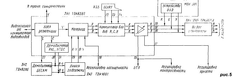
Encyclopedia of radio electronics and electrical engineering / Телевидение Extension The MRCC video path is assembled on six microcircuits: TDA8362, TDA8395, TDA4661 and three TDA6101Q. It includes a rejection node, signal demodulators of various broadcasting systems, a delay line, a matrix, an R, G, B input switch, an OSD device, and video amplifiers. The relationship of these devices is shown in Fig.5. In the video path, the video signal is converted into color difference and then into color signals.
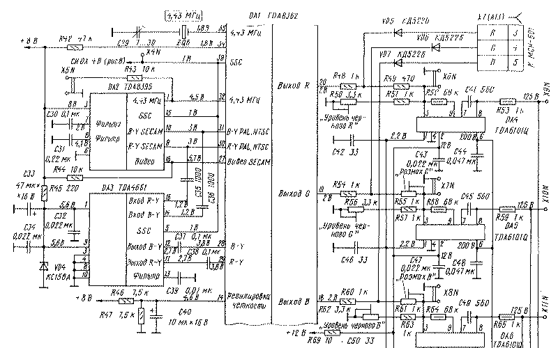
A feature of the TDA8362 microcircuit is the construction of notch and bandpass filters of the color path (flare filter, etc.) without external coils, while in the MTs-2/3/31 3USCT TVs, six or seven adjustable oscillatory circuits are used for this. If you do not take into account video amplifiers, then in the video path there are no elements at all to be configured. The rejection unit cuts out the color component C from the video signal - the frequency band occupied by the subcarriers of the color difference signals. Recall that in the NTSC system the subcarrier frequency is 3.58 MHz, in the PAL system it is 4.43 MHz. In the SECAM system, there are two subcarriers with frequencies of 4.25 and 4.406 MHz. Frequency determination, depending on the broadcasting system, occurs automatically in the node. Rejection depth - 20 dB, which provides effective cleaning of the luminance signal from the chrominance subcarriers with a minimum width of the cut out bandwidth. This enhances the clarity of the image. When a black-and-white image signal is received, the rejection unit recognizes it and turns off. The luminance Y component passes into the synchronization path and into the matrix. The color component is fed to the demodulators. The demodulator of PAL, NTSC signals is located in the DA1 chip. As a result of its work, color difference signals RY, BY are distinguished, which, through pins 30 and 31 of the microcircuit, come to the signal delay line by one line (DA3 microcircuit). In it, NTSC signals are filtered, and PAL signals are averaged over two lines following one after the other. From the output of the DA3 chip (pins 12 and 11), the processed signals RY, BY of the PAL and NTSC systems are again returned to the DA1 chip through pins 28 and 29. The SECAM signal demodulator is contained in the DA2 chip. Through pin 27 of the DA1 chip, component C of the SECAM system is fed to the DA2 chip, and from pin 32 of the DA1 chip, a signal with a frequency of 4.43 MHz, necessary for the operation of the demodulator, is supplied. The received color difference signals RY, BY of the SECAM system from pins 9 and 10 of the DA3 chip also pass to the delay line, where the correct sequence of direct and delayed lines is formed in each of the color difference signals. The signals RY, BY coming from the DA3 chip of all systems in the DA1 chip, after equalizing the time delays, enter the matrix, where, mixing with the brightness component Y, they are converted into color signals R, G, B. Through pins 22-24 of the DA1 chip, signals come to the switch R, G, B from an external source - a computer (see Fig. 3 and 4). The control of the switch is provided by the voltage of the blanking signal FB ("Window") supplied from the computer to output 21. If it is absent, signals from the matrix pass to the switch output, and at FB <5 V - from the computer. Then the signals R, G, B come to the output video amplifiers. Video amplifiers (VU) are high-voltage powerful operational amplifiers TDA6101Q. Their main advantage is broadband and the absence of powerful resistors in the output circuits (no more than 0,5 W). They have sensors of the automatic white balance system (ABB), but since the TDA8362 chip (unlike other modifications) does not contain the means to control the ABB system, this function is not used.
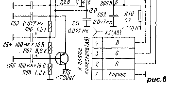
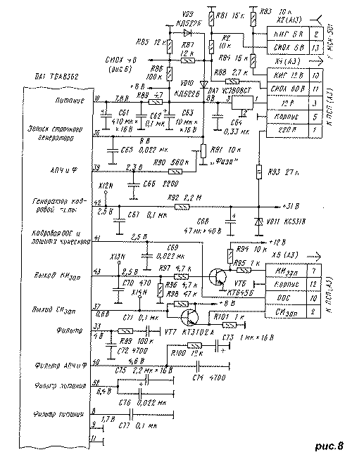
Let's consider the operation of the VU (Fig. 6) using the example of the passage of signal B. From the output 18 of the DA1 microcircuit to the input of the op-amp (pin 3) DA6, the signal B enters through the divider R60-R63. Resistor R62 "Black Level B" sets the constant component of the output signal equal to 125 V. Resistor R61 "Peak B" aligns the variable component of the signal B with the same value of the signal R. Resistor R63 is used when adjusting the white balance "in black" (at the blanking level kinescope rays), and resistor R61 - when adjusting the white balance "in light" (at the level of normal brightness). At the point of connection of resistors R60, R61 with MSN comes component B of the signal for displaying information on the screen (OSD system). At the connection point of resistors R61, R63, a deep negative feedback signal passes through resistor R64 from pin 9 of the DA6 chip. Resistor R65 protects the video amplifier from discharges occurring in the kinescope. Capacitor C49 corrects the frequency response of the amplifier at high frequencies. Capacitors C51 and C52 - filtering in the supply voltage circuits +12 and +220 V. Capacitor C50 - filtering in the circuit of the reference voltage +2.2 V, necessary to stabilize the operation of the amplifiers. It is formed by a stabilizer on the transistor VT5. The X8N control points are necessary when adjusting the purity of color and convergence of the kinescope beams. When they are closed, beam B is extinguished. Point X11N serves to check the level and shape of the signal supplied to the kinescope. Video signal amplifiers R and G are built similarly, except that there is no peak-to-peak regulator in the R path.
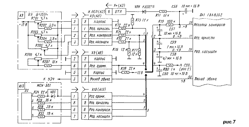
The circuits for connecting the adjustments of the image and sound parameters to the MRCC are shown in Fig. 7. Volume control in 3USTST is provided by changing the resistance of the resistor circuit R206, R207 in the control unit (A9), connected between the UPCHZ-1/2 microassembly in the MRK module and the common wire. When using the TDA8362 microcircuit, the adjustment occurs when the voltage at its pin 5 changes within 0.1 ... 3.9 V. To do this, if there is a SVP or USU, the R80C60R78 circuit is connected together with resistors R207, R206 in the control unit. Resistor R207 (it is designated as R33 in BU-3 / 3-1, R7 in BU-4, R6 in BU-5 and R15 in BU-14) must have a resistance of 1 kOhm. When using the MCH, the volume control circuit includes elements R80, C60 and a resistor R34 in the MCH. In this case, in the MSN, the VD5 diode is closed with a jumper, and the resistance of the resistors R28, R29 should be 18 kOhm. Brightness, contrast and saturation when using SVP and USU are still regulated by variable resistors R201, R203, R205 located on the front panel of the TV. Since the regulating voltage is removed from their engines in the range of 0 ... 12 V, and a signal of no higher than 1 V must be applied to the DA5 chip, voltage dividers R5R9, R72R73, R74R77 are connected after the contacts of the X75 (A76) socket. When using the MCH, all adjustments are made through the module from the remote control or from the keyboard on the front of the TV. All TV control resistors will be turned off. In both cases (when using SVP, USU or MSN), the control voltages of the adjustments are transmitted to pins 17, 25, 26 of the microcircuit through circuits that include filter capacitors C57-C59. When using SVP, USU, they stabilize the control voltage, and when working with the MSN, they average the pulse signals of variable duty cycle adjustments generated by the module. Through the elements VD8, R71, C56, the contrast control circuit is supplied with a beam current limiting voltage (ECL), which reduces the amplitude of the R, G, B signals entering the WU, with an increase in the total beam current above the norm. At any UVP, the color tone adjustment resistors are disabled. The synchronization path consists of horizontal and vertical sync selectors, horizontal scanning trigger pulse generators (SIapp) and vertical scan pulses. The horizontal sync selector separates the horizontal sync pulses from the luminance Y component of the video signal coming from the video input switch. The Y signal, the amplitude stabilization of which was provided in the radio path by an effective AGC and a white spot inversion unit, is limited by the maximum and minimum so that the horizontal and vertical blanking signals, as well as the "flashes" of the color synchronization signal, are guaranteed to be cut out at any range of the Y brightness component.
The cleaned horizontal sync pulses of stable amplitude are fed to the first loop of the PLL system, which corrects the frequency of the SI pulses based on them.app. The sync capture bandwidth of the first loop is +/-900 Hz, and the captured sync retention bandwidth is +/-1200 Hz, which is significantly better than the corresponding indicators (+/-700 Hz) for the K174XA11 chip used in the USR submodule of 3USCT TVs. The second loop of the horizontal PLL, as usual, ensures the stability of the position of the left vertical border of the image. Resistor R91 "Phase" (Fig. 8) allows you to correctly set the phase of the image. SI impulsesapp with an amplitude of 0.8 V from pin 37 of the DA1 microcircuit pass through the emitter follower on the VT7 transistor to pin 2 of connector X5 (A3) and then to the line scan module. Vertical scan control pulses are formed in the DA1 chip from a sequence of SI pulsesapp when dividing it by the number of lines in the half-frame of the image (determined in the process of identifying the coding system for color signals) with the correction of the origin of the frame sync pulses (FSI) coming from the frame sync selector. Such a construction facilitates the search for vertical sync pulses in a wide band (45 ... 64.5 Hz). As soon as 50 sequentially received frame sync pulses (FSI) are within the wide capture band, the system switches to a narrow band in which it will continue to work. If six consecutive KSI go beyond the narrow band, the device enters the mode of searching for them in a wide band. Vertical sweep sawtooth pulses (CST) with an amplitude of 1.25 ... 1.5 V are formed at pin 42 of the DA1 microcircuit by an integrating circuit R92C67, to which a +31 V voltage is applied, stabilized by a VD11 zener diode. The linearity of the pulses is improved by applying a personnel negative feedback (OOS) voltage with an amplitude of 1 V, which comes to pin 41 of the DA1 chip from the OOS sensor - a resistor included in the personnel deflecting coil circuit. In addition to improving the linearity of the CPT, the CNF sensor performs the function of monitoring the operation of the vertical scanning output stage. If the voltage on it is less than 1 V (an open in the chain of frame coils) or more than 4 V (the output stage is faulty), the outputs R, G, B of the DA1 chip are closed to avoid burning the kinescope.
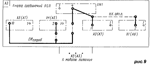
In 3USCT TVs, the frame signal is generated in the frame scan module MK-1-1 on resistor R27. In the PSP board (A3) it is available on pin 2 of connector X1 (A6) and on pin 11 of connector X3 (A7). To transfer it to the MRCC, you can use the SI circuit released with the introduction of the modulestrobe, connecting pin 10 of connector X5 (A1) and pins 4 of connectors X4 (A2) and XN1 on the PSP. All these circuits are shown in Figure 9. To implement the proposal, connect pin 11 of connector X3 (A7) and pin 4 of connector XN1 on the PSP with a jumper. Figure 9 shows a view of the board from the side of the printed conductors. The dashed line shows the jumpers located on the side of the sockets. In televisions with a TDA8362 chip, the TDA3651 / 54 (K1021XA8) or TDA3651Q / 54Q (K1051XA1) microcircuit, which has current control, is usually used in the vertical scan output stage. The frame trigger pulse transmitted from pin 43 of the TDA8362 chip to such an output stage is a current pulse with an amplitude of at least 1 mA during the forward path of the beam and several microamperes during the reverse stroke. It corresponds to the voltage at pin 43 with a level of 5 V for forward and 0.3 V for reverse, i.e. short retrace trigger pulses pointing down from the 5V level. In 3USCT TVs, the control of the MK-1-1 module is provided by positive (upward-directed) pulses for starting a vertical scan with an amplitude of 10 V. An amplifier is used to match the shape and amplitude of the pulses coming from pin 43 of the DA1 microcircuit with those required for the MK-1-1 module. inverter assembled on a transistor VT6 (Fig. 8).
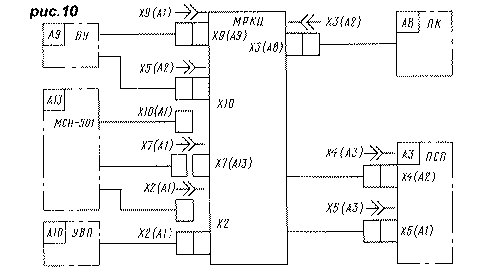
The connection diagram of the MRCC with the rest of the 3USST TV units is shown in Fig. 10. Before proceeding to the description of the module design, let's consider its possible modifications depending on the type of TV being upgraded and the wishes of its owner. 1. Channel selectors SK-M-24-2 and SK-D-24 will work successfully in MRCC, however, replacing them with more modern all-wave selectors SK-B-618, KS-V-73 and especially UV-917 will significantly increase the sensitivity of the TV, improve the signal-to-noise ratio and simplify the module due to the direct (without transistor VT1) connection of the selector with the filter ZQ1 (see Fig. 2). The presence of a combined antenna input for these selectors for MV and UHF eliminates the problem of connecting to the two antenna inputs of the 3USST TV of the distribution network of the collective reception.
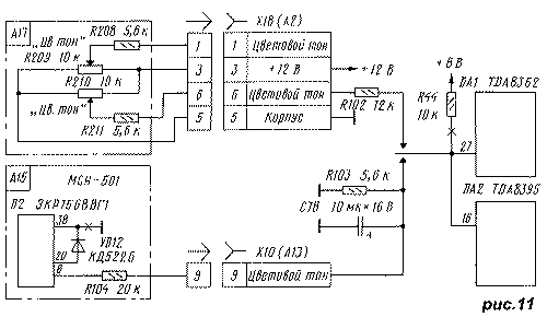
2. The list of color television systems processed by the TDA8362 chip is determined by the voltage at its pin 27. If it is more than +5 V (pin 27 is connected to the +44 V voltage conductor through resistor R8, as shown in Fig. 6), then only signals from SECAM systems are processed and PAL. If there is a need to process any of the NTSC systems, then the circuit for connecting output 27 of the microcircuit should be mounted in accordance with Fig. 11 by installing elements R102-R104, C78, VD12 and removing resistor R44. When using UVP types USU, SVP, the NTSC color tone control (in this system such an operational adjustment is necessary, since a change in the amplitude of the brightness signals causes a change in image color) is a variable resistor R211 (Fig. 11) - one of the two color tone controls installed on the case TV. When setting the MCH to adjust the NTSC color tone, the adjustment that is not used in the standard inclusion of the synthesizer is used, which is output to pin 6 of the D2 MCH chip. To do this, pin 6 of the D2 chip is connected to pin 9 of the X10 MCH connector through a 104 kΩ resistor R20. The TONE symbol will appear on the screen as an indication of the adjustment. If you wish, the designation can be replaced with the correct HUE (color) if you turn on the VD11 diode between pins 20 and 38 of the D2 MCH chip, unsoldering pin 38 from the common wire. All this will allow you to receive NTSC-4.43 signals from the video input. As for the signals of the NTSC-3.58 system received from the antenna input, their processing requires a serious change in the radio path. It is necessary to include in it a band-pass and notch filters at a frequency of 4.5 MHz. Parallel connection of three notch filters between the transistor VT2 and pin 13 of the DA1 chip (see Fig. 2) will result in a too wide frequency band being cut out in the video signal, which will degrade the image clarity. To solve this problem, PANASONIC TVs based on the MX3C chassis [5] use a special microcircuit that recognizes the standard and includes only one required notch filter. Its addition would significantly complicate the MRCC, and therefore is not recommended. 3. The 2USCT TV uses the same modules as the 3USCT TV. The pinouts of all connectors are the same, and the installation of MRCC in these TVs does not cause additional problems. 4. This is not the case with the 4USCT series. Before manufacturing a module for them, it is necessary to compare the pinout of the module connectors with the pinout of the mating parts of the TV and make the necessary changes to the MRCC. The dimensions of the module board given below correspond to the dimensions of the 3USCT cassette and may not match the dimensions of the chassis of the TV being upgraded. it may be necessary to re-layout the MRCC board. It is impossible to give more specific recommendations, since, unlike 3USCT, the circuit diagrams and printed circuit boards of 4USCT TVs from different factories are not unified and differ greatly from each other. It is proposed to be guided by the factory scheme of the upgraded TV and the reference book [6]. 5. In the TV UPIMTST, the MRCTS module can well be used to replace the BOS signal processing unit, provided it is supplemented with the UM1-3 (UZCH) module and the kinescope beam damping cascade (both are on the BOS). Another (in relation to 3USTST) size of the cassette requires an increase in the size of the board without changing the pattern of printed conductors. With the simultaneous replacement of the selector SK-V-1 (Kу which is lower than that of SK-M-24-2) to a more modern one, and a UVP of the SVP-4 type on the MSN in UPIMTST can get all the functions of a fifth-generation TV. 6. In the transition from UPIMCT to 3USCT model 3USCT-P (aka 4UPIMCT), the MRCC module could replace the entire BROS scanner and signal processing board, on which the radio channel, brightness and color channels are located. It has a selector SK-M-24, modules UM1-1, UM1-2, UM1-3, UM1-4, UM2-1-1, UM2-2-1, UM2-3-1, UM2-4-1 , M2-5-1. All of them, except for the selector and UM1-3, are not needed. The M3-1-1 synchronization module installed on the BROS scan board is also not needed. Replacing this set of modules with a new one (MRCC) is, of course, possible and desirable, but it requires serious alterations in the module and the remaining BROS board due to a completely different system of interboard connections and is not recommended. Literature 4. Peskin A., Konnov A. TV sets of foreign companies. Device, adjustment, repair. Series "Repair", issue 17 - M .: Solomon, 1998.
Publication: N. Bolshakov, rf.atnn.ru
Alcohol content of warm beer
07.05.2024 Major risk factor for gambling addiction
07.05.2024 Traffic noise delays the growth of chicks
06.05.2024
▪ Transcend introduces copy-protected memory cards ▪ Flexible material for pulse sensors ▪ The chicken's speech is deciphered
▪ Modeling section of the site. Selection of articles ▪ article by Philip Sidney. Famous aphorisms ▪ article How does coffee affect people? Detailed answer ▪ article Wormwood annual. Legends, cultivation, methods of application ▪ article Keypad. Encyclopedia of radio electronics and electrical engineering ▪ article Regeneration of galvanic cells. Encyclopedia of radio electronics and electrical engineering
Home page | Library | Articles | Website map | Site Reviews
www.diagram.com.ua |

 Leave your comment on this article: