|
|


 Arabic
 Bengali
 Chinese
 English
 French
 German
 Hebrew
 Hindi
Hindi Italian
 Japanese
 Korean
 Malay
Malay Polish
 Portuguese
 Spanish
 Turkish
 Ukrainian
 Vietnamese
|
ENCYCLOPEDIA OF RADIO ELECTRONICS AND ELECTRICAL ENGINEERING Microcontroller PIC16C84. Short description. Encyclopedia of radio electronics and electrical engineering
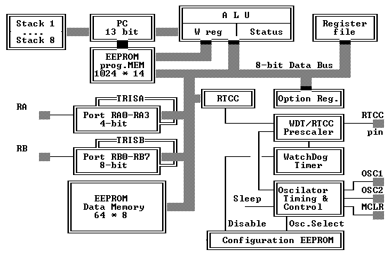
Encyclopedia of radio electronics and electrical engineering / Microcontrollers This description does not claim to be complete and contains a number of errors and typos. Complete documentation can be obtained from Microchip distributors, whose addresses are given at the end of the file. Introduction PIC16C84 belongs to the family of CMOS microcontrollers. It differs in that it has an internal 1K x 14 bit EEPROM for programs, 8-bit data and 64 bytes EEPROM of data memory. At the same time, they are characterized by low cost and high performance. Users who are familiar with the PIC16C5X family can see a detailed list of differences between the new and previously produced controllers. All instructions are one word (14 bits wide) and execute in one cycle (400 ns at 10 MHz), except jump instructions, which are executed in two cycles (800 ns). The PIC16C84 has a four-source interrupt and an eight-level hardware stack. The peripherals include an 8-bit timer/counter with an 8-bit programmable prescaler (actually a 16-bit timer) and 13 bidirectional I/O lines. The high load capacity (25mA max sink, 20mA max sink) of the I/O lines simplifies external drivers and thus reduces overall system cost. Development based on PIC16C84 controllers is supported by assembler, software simulator, in-circuit emulator (Microchip only) and programmer. The PIC16C84 series is suitable for a wide range of applications from high speed automotive and electric motor control circuits to cost effective remote transceivers, indicating instruments and communication processors. The presence of ROM allows you to adjust the parameters in application programs (transmitter codes, engine speeds, receiver frequencies, etc.). The small package sizes, both conventional and surface mount, make this series of microcontrollers suitable for portable applications. The low price, economy, speed, ease of use, and I/O flexibility make the PIC16C84 attractive even in areas where microcontrollers have not been used before. For example, timers, replacing hard logic in large systems, coprocessors. It should be added that the PIC16C84's built-in EEPROM programmer makes it easy to customize the program and data for specific requirements even after assembly and testing is completed. This possibility can be used both for replication and for entering calibration data after the final testing. Features Overview - only 35 simple commands; - all commands are executed in one cycle (400ns), except for transition commands -2 cycles; - operating frequency 0 Hz ... 10 MHz (min 400 ns command cycle) - 14 - bit commands; - 8 - bit data; - 1024 x 14 electrically reprogrammable program memory on a chip (EEPROM); - 36 x 8 general use registers; - 15 special hardware registers SFR; - 64 x 8 electrically reprogrammable EEPROM memory for data; - eight-level hardware stack; - direct, indirect and relative addressing of data and commands; - four interrupt sources: . external input INT . RTCC timer overflow . interrupt on change of signals on the lines of port B . upon completion of writing data to the EEPROM memory Peripherals and I/O - 13 I / O lines with individual settings; - Sink/sink current to drive LEDs . max incoming current - 25 mA . max flowing current - 20 mA - 8-bit RTCC timer/counter with 8-bit programmable prescaler; - automatic reset when turned on; - the timer of inclusion at reset; - generator start timer; - Watchdog WDT timer with its own built-in generator providing increased reliability; - EEPROM security bit to protect the code; - economical SLEEP mode; - user-selectable bits to set the drive mode of the built-in oscillator: - RC generator : RC - conventional quartz resonator : XT - high frequency quartz resonator : HS - economical low-frequency crystal : LP - built-in EEPROM programming device for program and data memory; only two legs are used. CMOS technology - economical high-speed CMOS EPROM technology; - static principle in architecture; - wide range of supply voltages and temperatures: . commercial: 2.0 ... 6.0 V, 0...+70C . industrial: 2.0 ... 6.0 V, -40...+70С . automotive: 2.0 ... 6.0 V, -40...+125С - low consumption . 3 mA typical for 5V, 4MHz . 50 µA typical for 2V, 32kHz . 26µA typical for SLEEP mode at 2V. Structural diagram PIC16C84
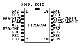
The architecture is based on the concept of separate buses and memory areas for data and commands (Harvard architecture). The data bus and data memory (RAM) are 8 bits wide, and the program bus and program memory (ROM) are 14 bits wide. This concept provides a simple yet powerful instruction set designed so that bit, byte, and register operations operate at high speed and overlap in instruction fetch and execution cycle times. The 14-bit program memory width allows a 14-bit instruction to be fetched in one cycle. The two-stage pipeline provides simultaneous fetching and execution of an instruction. All instructions are executed in one cycle, excluding jump instructions. The PIC16C84 has 1K x 14 program memory located on-chip. The executable program can only reside in the built-in ROM. Differences between PIC16C84 and PIC16C5x 1. Command length increased to 14 bits. This allows you to organize ROM and RAM with an increased page size: (2K bytes instead of 512 bytes), (128 bytes instead of 32 bytes), respectively. 2. The program counter high register (PCLATH) controls page switching in program memory. The page selection bits PA2, PA1, PA0, which were used for this in the PIC16C5X crystal, are removed from the STATUS register. 3. Memory paging and STATUS register have been modified. 4. Added four new commands: RETURN, RETFIE, ADDLW, SUBLW. The two commands TRIS and OPTION are no longer needed, but are retained for software compatibility with the PIC16C5X. 5. The OPTION and TRIS registers are made addressable by number. 6. Added the ability to work on interrupts. Vector=0004h. 7. Stack size increased to eight levels. 8. Power-on reset address changed to 0000h. 9. Five different types of resets (exits from the SLEEP mode) are recognized. Register initialization changed. They are set differently, depending on the type of reset. 10. Added exit from SLEEP mode via interrupt. 11. For more reliable startup, the following hardware delays have been added: start-up timer (OST) and power-on timer (PWRT). These timers can be used selectively to avoid unnecessary delays, both when turning on and when exiting SLEEP mode. 12. Port B has active loads and an interrupt when input signals change. 13. The RTCC leg is aligned with the port leg (RA4). 14. Register address 07h (port C) does not exist and is not a general purpose register. 15. The register FSR (f4), which stores the pointer with indirect addressing, has become eight bits wide. 16. Implemented built-in EEPROM programming machine. The user can program the PIC16C84 using only five pins: Vdd, Vss, /MCLR/Vpp, RB6(clock), RB7(data in/out). Transition from PIC16C5x to PIC16C84 To convert the code written for PIC16C5X to code for PIC16C84, the user must perform the following steps: 1. Replace operations for selecting pages of program memory (bits PA2, PA1, PA0) with CALL, GOTO commands. 2. Review all computed jump operations (write to PC or add to PC, etc.) and make sure the page bits are set correctly for the new chip as well. 3. Eliminate data memory page switching. Redefine variables and reallocate memory for them. 4. Check the entry in the STATUS, OPTION, FSR registers, because they are slightly modified. 5. Change the power-on reset vector to 0000h. 6. Note that address 07h is a non-existent data memory address. Enclosure types and versions Package designations for PIC16C8x crystals. The package type is indicated in the Marking when ordering microcircuits. Cases come with only 18 Pins. PDIP - Plain plastic two-row case. Used for OTP EPROM versions of crystals. SOIC - Small DIP Surface Mount Package Chip designs come in three types: commercial, industrial, and automotive. Their main difference is in the temperature range and operating voltage. Commercial execution Operating temperature 0 ... +70 C Operating voltage 3.0 ... 5.5 V Industrial version Operating temperature -40 .... +85 C Operating voltage 3.0 ... 5.5 V Vehicle version Operating temperature -40 ... +125 C Operating voltage 3.0 ... 5.5 V Marking when ordering The designation of microcircuits consists of the following fields: <Company number>-<Generator frequency><Temperature range>/<Body><Note> <company number may be>: PIC16C84 - Vdd range 4...6 V PIC16LC84 Vdd range 2...6 V <Originator frequency>: 04 ---> 4 mHz 10 ---> 10mHz The temperature range is: - from 0С to +70С I from -40С to +85С E from -40С to +125С The body is marked: P - regular plastic DIP SO-300 mil SOIC EXAMPLES: PIC16C84-04/Pxxx 4 mHz, commercial version in PDIP package, Vdd normal range, mask ROM with xxx program PIC16LC84-04I/SO 4 mHz, industrial version, extended power range, case=SOIC PIC16C84-10E/P car version, 10 mHz, PDIP, typ. food Leg layout For the function of the pins, see "Pin Designations" or the Block Diagram. For PDIP enclosure types, etc., see Enclosures.
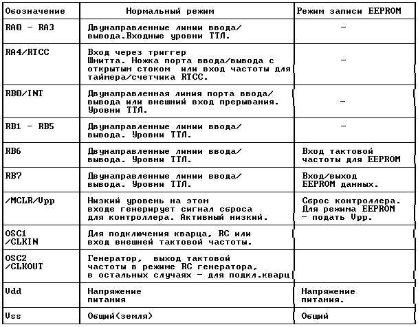
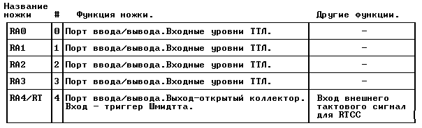
The purpose of the legs Designations of legs and their functional purpose.
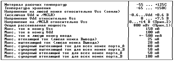
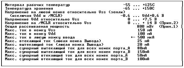
Maximum values of electrical parameters Parameters outside these limits may damage the chip. Operating the crystal at its limit values for a long time will affect its reliability.
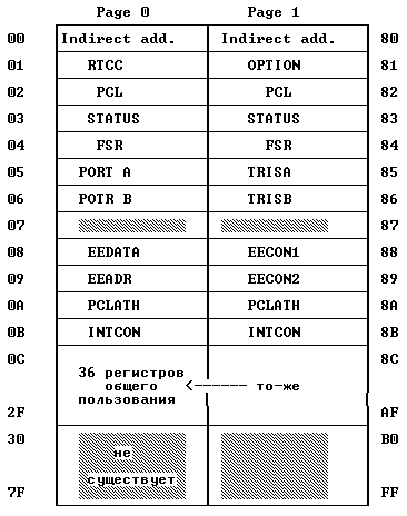
Notes: 1. Total power dissipation must not exceed 800mW for each enclosure. The dissipated power is calculated using the following formula: Pdis= Vdd(Idd - Sum(Ioh)) + Sum ((Vdd - Voh)Ioh) + Sum (Vol Iol) 2. Dropping the voltage on the /MCLR pin below Vss(ground) will induce high currents, greater than 80mA, and may damage this line. Therefore, we recommend that you apply signals to the /MCLR pin through a 50-100 ohm terminating resistor. Overview of registers and RAM The RAM area is organized as 128 x 8. The RAM cells can be addressed directly or indirectly through the FSR pointer register (04h). This also applies to the EEPROM of the constant data memory.
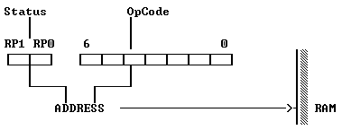
The status register (03h) contains page select bits that allow access to four pages of future revisions of this chip. However, for the PIC16C84, the data memory only exists up to address 02Fh. The first 12 addresses are used to house the special purpose registers. Registers with addresses 0Ch-2Fh can be used as general purpose registers, which are static RAM. Some special purpose registers are duplicated on both pages, and some are located separately on page 1. When page 1 is set, accessing addresses 8Ch-AFh effectively addresses page 0. Registers can be addressed directly or indirectly. In both cases, up to 512 registers can be addressed. Direct Addressing When direct 9-bit addressing is performed, the lower 7 bits are taken as the direct address from the opcode and the two page pointer bits (RP1,RP0) from the status register (03h).
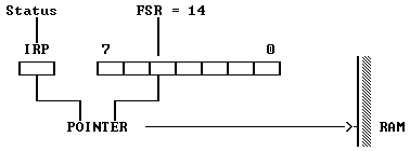
indirect addressing f4 - Indirect address pointer Any instruction that uses f0 (address 00) as a register actually accesses a pointer that is stored in the FSR (04h). Reading f0 itself indirectly will result in 00h. Writing to register f0 will implicitly look like Nop, but the status bits can be changed. The required 9-bit address is formed by combining the contents of the 8-bit FSR register and the IRP bit from the status register.
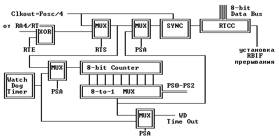
Note that some special function registers are located on page 1. To address them, you must additionally set the RP0 bit in the status register to one. RTCC timer/counter The block diagram for enabling RTCC is shown below. It contains the element "MUX" - this is an electronic switch.
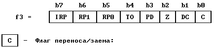
The timer mode is selected by resetting the RTS bit in the OPTION register to zero. In timer mode, the RTCC will be incremented from the INTERNAL frequency source - every command cycle (no prescaler). After writing information to RTCC, it will start incrementing after two instruction cycles. This happens with all instructions that write or read-modify-write f1 (eg MOVF f1, CLRF f1). This can be avoided by writing an adjusted value to RTCC. If RTCC needs to be checked for zero without stopping the count, use the MOVF f1,W instruction. The counter mode is selected by setting the RTS bit in the OPTION register to one. In this mode, RTCC will be incremented by either a rising or falling edge on the RA4/RTCC pin from EXT events. The direction of the edge is determined by the RTE control bit in the OPTION register. With RTE=0, a rising edge will be selected. The limiter can be used with either RTCC or Watchdog timer. The divider connection option is controlled by the PSA bit in the OPTION register. With PSA=0, the divider will be connected to the RTCC. The content of the divider is not available to the program. Division factor - programmable. An RTCC interrupt is generated when the RTCC timer/counter overflows on the transition from FFH to 00h. The RTIF request bit in the INTCON<2> register is then set. This interrupt can be masked by the RTIE bit in the INTCON<5> register. The RTIF request bit must be cleared by software when handling the interrupt. An RTCC interrupt cannot wake the processor from SLEEP because the timer does not function in this mode. Timer problems Problems can arise when counting external signals. These signals are gated by an internal clock signal, see the SYNC diagram. There is some delay between the rising edge of the input signal and the RTCC increment time. Gating is done after the limiter. The limiter output is polled twice during each command cycle to determine the rising and falling edges of the input signal. Therefore, the Psout signal must be high and low for at least two clock periods. When the limiter is not used, Psout repeats the input signal, so the requirements for it are as follows: Trth= RTCC high time >= 2tosc+20ns Trtl= RTCC low time >= 2tosc+20ns. When the limiter is used, the RTCC input is divided by the number set in the divider counter. The signal after the limiter is always symmetrical. Psout high time = Psout low time = NTrt/2, where Trt is the RTCC input period, N is the value of the divider counter (2,4...256). In this case, the requirements for the input signal can be expressed as follows: NTrt/2 >= 2tosc +20ns or Trt >= (4tosc + 40ns)/N. When a limiter is used, the low and high signal levels at its input must be at least 10 ns. Thus, the general requirements for an external signal when a divider is connected are as follows: Trt= RTCC period >= (4tosc + 40ns)/N Trth = RTCC high time >= 10ns Trtl = RTCC low time >= 10ns. Because the limiter output is clocked by the internal clock, there is a slight delay between the rising edge of the external clock and the actual RTCC increment time. This delay is between 3tosc and 7tosc. Thus, the measurement of the interval between events will be performed with an accuracy of 4tosc (+-400ns at 10 MHz quartz). Status register Register (f3) contains the ALU's arithmetic flags, controller reset state, and page select bits for data memory. (f3) is available to any command just like any other register. However, the TO and PD bits are set by hardware and cannot be written to a status by software. This should be kept in mind when executing a command using the status register. For example, the CLRF f3 instruction will set all bits to 1 except for the TO and PD bits, and then set the Z=3 bit. After executing this command, the status register may not have a zero value (due to the TO and PD bits) f000=100??XNUMX. Therefore, it is recommended to use only BCF, BSF, MOVWF bit setting commands to change the status register, which do not change the rest of the status bits. The effect of all commands on the status bits can be seen in the "Description of commands". Software Status Flags The location of the flags in the status register is as follows:
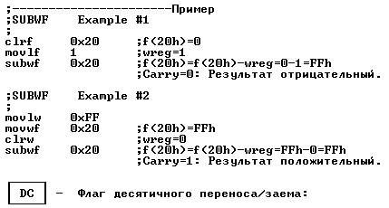
For ADDWF and SUBWF commands. This bit is set if the most significant bit operation results in a carry. Subtraction is carried out by adding the additional code of the second operand. When executing shift instructions, this bit is always loaded from the LSB or MSB of the source being shifted.
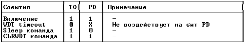
For ADDWF and SUBWF commands. This bit is set if the fourth bit operation results in a carry. The mechanism for setting the decimal carry bit "DC" is the same, except that the carry from the fourth bit is monitored. Z - Zero result flag: Set if the result of an arithmetic or logical operation is zero. PD - Power Down (data storage mode) : Set to "1" at power-up or CLRWDT command. Reset to "0" by the SLEEP command. TO - Time out. Watchdog timer activation flag: Set to "1" on power-up and CLRWDT, SLEEP commands. Resets to "0" when the WDT timer expires. RP1, RP0 - Data memory page selection bits for direct addressing: RP1,RP0: 00= Page 0 (00h-7Fh) 01= Page 1 (80h-FFh) 10= Page 2 (100h-17Fh) 11= Page 3 (180h-1FFh) Each page contains 128 bytes. The PIC16C84 chip uses only RP0. In this chip, RP1 can be used simply as a general purpose read/write bit. However, it must be remembered that in subsequent developments it will be used. IRP - Data memory page selection bit for indirect addressing: IRP0: 0= Pages 0,1 (00h-FFh) 1= Page 2,3 (100h-1FFh) This bit in the PIC16C84 crystal does not make sense to use. Therefore, it can be used as a general purpose read/write bit. However, we must remember that in subsequent developments it will be used. Hardware Status Flags Hardware status bits TO (Time Out) and PD (Power Down). The state of the status register bits "TO" and "PD" can determine what caused the "Reset": - by simply turning on the power, - activation of the watchdog timer, - exiting the sleep mode as a result of the watchdog timer being triggered, - by external signal /MCLR. Only the following events can affect the state of these bits:
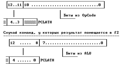
Note: The TO and PD bits remain current until one of the events listed in the table occurs. "0" - A low-level pulse at the input of the /MCLR crystal does not change the state of the TO and PD bits. Organization of the built-in ROM The program counter in the PIC16C84 is 13 bits wide and can address 8Kx14 bits of program memory. However, physically there is only 1Kx14 memory on the chip (addresses 0000h-03FFh). Addressing addresses above 3FFh is actually addressing the same first kilobyte. The reset vector is located at address 0000h, the interrupt vector is located at address 0004h. The EEPROM of the PIC16C84 is designed for a limited number of erase/write cycles. To write to program memory, the crystal must be put into a special mode in which the programming voltage Vprg is applied to the /MCLR pin, and the power supply Vdd must be in the range of 4.5V ... 5.5V. The PIC16C84 is not suitable for applications where the program is modified frequently. Writing to program memory is done bit by bit, sequentially using only two pins. PC and ROM addressing (f2). Program counter The width of the program counter is 13 bits. The Program Counter Low Byte (PCL) is read/write and is located in register 02h. The program counter high byte (PCH) cannot be directly read or written. The high byte of the program counter can be written to via the PCLATH register, whose address is 0Ah. Depending on whether a new value is loaded into the program counter during CALL, GOTO instructions, or the low byte of the program counter (PCL) is being written to, the high bits of the program counter are loaded from PCLATH in different ways, as shown in the figure. Case of GOTO, CALL commands
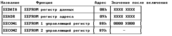
Stack and Returns from Subroutines The PIC16C84 crystal has an eight-level 13-bit wide hardware stack. The stack area belongs to neither the program area nor the data area, and the stack pointer is not accessible to the user. The current value of the program counter is pushed onto the stack when a CALL instruction is executed or an interrupt is processed. When a RETLW, RETFIE, or RETURN instruction is executed from a subroutine), the contents of the stack are popped into the program counter. The PCLATH register (0Ah) is not changed by stack operations. Data in EEPROM Non-volatile EEPROM data memory. EEPROM data memory allows you to read and write a byte of information. When a byte is written, the previous value is automatically erased and new data is written (erase before write). All these operations are performed by the built-in EEPROM writer. The contents of this memory are retained when the power is turned off. The PIC16C84 crystal has a 64x8 bit EEPROM data memory that allows writing and reading during normal operation (over the entire supply voltage range). This memory does not belong to the RAM register area. It is accessed through two registers: EEDATA <08h>, which contains eight-bit data for reading / writing and EEADR <09h>, which contains the address of the cell being accessed. Additionally, there are two control registers: EECON1 <88h> and EECON2 <89h>. When reading data from the EEPROM memory, write the desired address to the EEADR register and then set the RD EECON1<0> bit to one. The data will appear in the next command cycle in the EEDATA register and can be read. The data in the EEDATA register is latched. When writing to EEPROM memory, you must first write the required address to the EEADR register and data to the EEDATA register. Then execute a special sequence of commands that produces direct recording: movlv 55h movwf EECON2 movlv AH movwf EECON2 bsf EECON1,WR ;set WR bit, start recording During the execution of this section of the program, all interrupts must be disabled in order to accurately execute the timing diagram. Recording time - approximately 10ms. Actual write time will vary depending on voltage, temperature, and individual crystal properties. At the end of the write, the WR bit is automatically reset to zero, and the EEIF write completion flag, which is also an interrupt request, is set. To prevent accidental writes to data memory, a special WREN bit is provided in the EECON1 register. It is recommended to keep the WREN bit off, except when the data memory needs to be refreshed. Moreover, the code segments that set the WREN bit and those that perform the write should be stored at different addresses to avoid accidentally executing both of them when the program crashes. EEPROM control Control registers for EEPROM
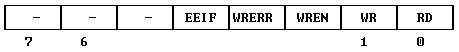
EECON1 and EECON2 registers The EECON1 register (address 88h) is a five bit wide control register. The lower five bits are physically present, while the upper three bits are always read as `0`. Register EECON1 Address 88h Reset at power on - 0000X000
The RD and WR control bits trigger reads and writes, respectively. They can only be set programmatically. Cleared by hardware when read/write operations are completed. Disabling the software reset of the WR bit prevents the write from ending prematurely. RD - Read bit. RD =1 : Starts reading the EEPROM data memory. Reading takes one cycle. Installed by software. Reset by hardware. WR - Write bit. WR =1 : Starts writing to EEPROM data memory. Installed by software. Reset by hardware. WREN - EEPROM write enable bit. WREN = 1: Write enabled. WREN = 0: Write disabled. After the power is turned on, WREN is reset to zero. The WRERR error flag is set when the write process is interrupted by the /MCLR reset signal or the reset signal from the WDT timer. We recommend that you check this WRERR flag and, if necessary, overwrite data whose data and address are stored in the EEDATA and EEADR registers. WRERR - Write error flag. WRERR = 1: The flag is set when a write operation is aborted by the /MCLR reset signal (during normal mode or SLEEP mode) or by the WDT reset signal during normal mode. The EEIF flag is set when the embedded automaton completes writing to data memory. It must be reset by software. EEIF - Write Completion Flag. EEIF = 1: The flag is set when the write is completed. The corresponding interrupt enable bit is EEIE in the INTCON register. Organization of interrupts Interrupts in the PIC16C84 can come from four sources: - external interrupt from pin RB0/INT, - RTCC counter/timer overflow interrupt, - interruption at the end of writing data to EEPROM - interrupt from changing the signals on the pins of the port RB<7:4>. All interrupts have the same vector/address - 0004h. However, in the interrupt control register INTCON it is written: - from which source the interrupt request was received. Written by the corresponding bit-flag. Such an interrupt can be masked individually or by a common bit. The only exception is the EEPROM write end interrupt. This flag is in another EECON1 register. The GIE General Interrupt Enable/Disable bit (INTCON <7>) enables (if=1) all individually unmasked interrupts or disables (if=0) them. Each interrupt can be additionally enabled/disabled by setting/clearing the corresponding bit in the INTCON register. The GIE bit is set to zero on reset. When an interrupt is processed, the GIE bit is set to zero to disable further interrupts, the return address is pushed onto the stack, and address 0004h is loaded into the program counter. Interrupt response time for external events, such as an interrupt from the INT pin or port B, is approximately five cycles. This is one cycle less than for internal events such as an overflow interrupt from the RTCC timer. The reaction time is always the same. In an interrupt handler, the source of the interrupt can be determined by the corresponding bit in the flags register. This flag bit must be cleared by software within a subroutine. The interrupt request flags are independent of the corresponding mask bits and the GIE general mask bit. The interrupt return instruction RETFIE terminates the interrupt routine and sets the GIE bit to enable interrupts again. Register of queries and masks Interrupt control register and its bits
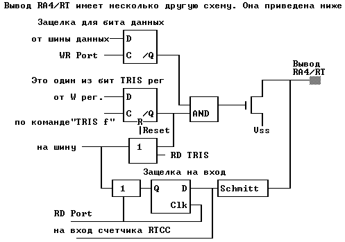
Address: 0bh Value at reset= 0000 000? RBIF - Change interrupt flag on the RB port. The flag is set when the signal at the RB<7:4> input changes. The flag is reset programmatically. INTF - Interrupt flag INT. The flag is set when the INT pin receives a signal from an external interrupt source. Reset by software. RTIF - RTCC Overflow Interrupt Flag. The flag is set when RTCC overflows. The flag is reset programmatically. RBIE - RBIF interrupt enable/disable bit. RBIE = 0 : disable RBIE interrupt RBIE = 1 : enable RBIE interrupt INTE - Bit enable/disable INT interrupt. INTE = 0 : disable INT interrupt INTE = 1 : enable INT interrupt RTIE RTIF interrupt enable/disable bit. RTIE = 0 : disable RTIE interrupt RTIE = 1 : enable RTIE interrupt EEIE - EEPROM write interrupt enable/disable bit. EEIE = 0 : disable EEIF interrupt EEIE = 1 : enable EEIF interrupt GIE All interrupt enable/disable bit. GIE = 0 : disable interrupts GIE = 1 : enable interrupts It resets automatically under the following circumstances: - power on. - by external signal /MCLR during normal operation. - by external signal /MCLR in SLEEP mode. - at the end of the WDT timer delay during normal operation. - at the end of the WDT timer delay in SLEEP mode. External interrupt An external interrupt on the RB0/INT pin is triggered on either a rising edge (if bit6 INTEDG=1 in the OPTION register) or a falling edge (if INTEDG=0). When a rising edge is detected on the INT pin, the INTF request bit is set (INTCON <1>). This interrupt can be masked by setting the INTE control bit to zero (INTCON <4>). The INTF request bit must be cleared by the interrupt program before the interrupt is enabled again. An INT interrupt can wake the processor from SLEEP mode if the INTE bit was set to one before entering this mode. The state of the GIE bit also determines whether the processor will jump to the interrupt routine after waking up from SLEEP mode. RTCC interrupt An RTCC counter overflow (FFh->00h) will set the RTIF request bit (INTCON<2>). This interrupt can be enabled/disabled by setting/clearing the RTIE mask bit (INTCON<5>). Resetting the RTIF request is up to the processing program. RB port interrupt Any change to the signals on the four inputs of the RB<7:4> port will set the RBIF bit (INTCON<0>). This interrupt can be enabled/disabled by setting/clearing the RBIE mask bit (INTCON<3>). Resetting the RBIF request is up to the processing program. EEPROM interrupt EEPROM write end interrupt request flag, EEIF (EECON1<4>), is set when automatic data writing to EEPROM is completed. This interrupt can be masked by resetting the EEIE bit (INTCON<6>). Resetting the EEIF request is up to the handler. Overview of registers/ports The crystal has two ports: a 5-bit RA port and an 8-bit RB port with bit-by-bit individual setting for input or output. Port A Line Diagram Port A is a 5 bit wide port, corresponding to the pins of the RA<4:0> chip. The RA<3:0> lines are bidirectional and the RA4 line is an open-drain output. Port A register address is 05h. Port A's TRISA control register is located on the first page of registers at address 85h. TRISA<4:0> is a 5 bit wide register. If a bit in the TRISA control register is set to one, then the corresponding line will be set to input. Zero switches the line to output and simultaneously outputs the contents of the corresponding latch register to it. Below is the diagram of ports RA0..RA3
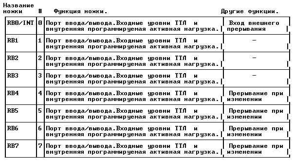
Port B Line Diagram Port B is a bidirectional port, eight bits wide (register address 06h). Pertaining to port B, the TRISB control register is located on the first page of registers at address 86h. If the control TRISB bit of the register is set to one, then the corresponding line will be set to input. Zero switches the line to output and simultaneously outputs the contents of the corresponding latch register to it. Each pin of port B has a small resistive load (about 100µA) on the power line. It is automatically disabled if this pin is programmed as an output. Moreover, the RBPU OPTION<7> control bit can disable (RBPU=1) all loads. A power-on reset also turns off all loads. The four lines of port B (RB<7:4>) have the ability to trigger an interrupt when the signal value changes on any of them. If these lines are configured for input, they are polled and latched into the Q1 read loop. The new value of the input signal is compared with the old value in each instruction cycle. If the value of the signal on the leg and in the latch does not match, a high level is generated. The outputs of the "mismatch" detectors RB4, RB5, RB6, RB7 are ORed and generate an RBIF interrupt (stored in INTCON<0>). Any line configured as an output does not participate in this comparison. An interrupt can wake the crystal from SLEEP mode. In the interrupt handler, reset the interrupt request in one of the following ways: 1) Disable interrupts by clearing the RBIE bit INTCON<3>. 2) Read port B. This will end the compare state. 3) Clear the RBIF INTCON<0> bit. Mismatch interrupts and software-settable internal active loads on these four lines can provide a simple interface, such as a keyboard, with keystroke wake-up from SLEEP mode. Leg RB0 is combined with the external interrupt input INT. Name
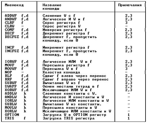
Port issues Problems when organizing bidirectional ports -Some commands are internally executed as read+write. For example, the BCF and BSF instructions read the entire port, modify one bit, and output the result back. This is where caution is needed. For example, the BSF instruction for bit 5 of register f6 (port B) first reads all eight bits. Bit 5 is then manipulated and the new value of the byte is written in its entirety to the output latches. If another bit of register f6 uses i as bidirectional I/O (say bit 0) and is currently defined as input, the input on that pin will be read and written back to that pin's output latch, overwriting its previous state. As long as this pin remains in input mode, no problems arise. However, if line 0 later switches to output mode, its state will be undefined. External current sources ("mounting AND", "mounting OR") should not "lean" on the leg operating in the output mode. The resulting large currents can damage the crystal. Serial access to I/O ports Writing to the output port occurs at the end of the command cycle. But when reading, the data must be stable at the beginning of the instruction cycle. Be careful with reads immediately following writes to the same port. Here it is necessary to take into account the inertia of establishing the voltage at the terminals. A software delay may be required to allow the voltage on the pin (depending on the load) to stabilize before the next read command is executed. Overview of commands and symbols Each PIC16C84 command is a 14-bit word, which is divided by meaning into the following parts: - 1. operation code, -2. a field for one or more operands that may or may not participate in this instruction. The PIC16C84 instruction set includes byte-oriented instructions, bit-oriented instructions, constant operations, and control transfer instructions. For byte-oriented commands, "f" denotes the register to operate on; "d" - bit determines where to put the result. If "d"=0 then the result will be placed in the W register, with "d"=1 the result will be placed in the "f" mentioned in the command. For bit-oriented instructions, "b" indicates the number of the bit involved in the instruction, and "f" is the register in which this bit is located. For transfer commands and constant operations, "k" denotes an eight or eleven bit constant. All commands are executed within one command cycle. In two cases, the execution of the instruction takes two instruction cycles: -1. condition check and jump, -2. change program counter as a result command execution. One command cycle consists of four periods of the generator. Thus, for a 4 MHz oscillator, the command cycle execution time will be 1 µs. Byte oriented commands
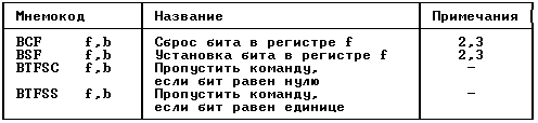
Bit oriented commands
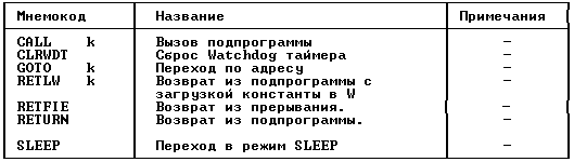
Transitions
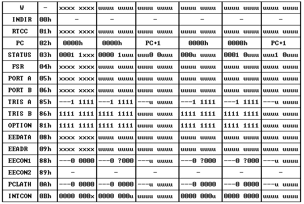
Notes and explanations Note 1: The TRIS and OPTION commands have been placed in the command list for compatibility with the PIC16C5X family. Their use is not recommended. On the PIC16C84, the TRIS and OPTION registers are read/write as regular numbered registers. Be warned that these commands may not be supported in future PIC16CXX developments. Note 2: When an I/O register is modified, such as MOVF 6,1, the value used for modification is read directly from the chip pins. If the output latch value for a pin programmed to output is "1", but the external signal on that pin is "0" due to "bulging" outside, then "0" will be read. Note 3: If the operand of this instruction is register f1 (and d=1 if allowed), then the divisor, if connected to RTCC, will be set to zero. Reset conditions In PIC16C84, there are differences between reset options: 1) Power-on reset. 2) External reset /MCLR during normal operation. 3) External reset /MCLR in SLEEP mode. 4) Reset at the end of the WDT timer delay during normal operation. 5) Reset at the end of the WDT timer delay in SLEEP mode. Some of the special registers are not initialized when reset. They have a random state at power-up and do not change with other types of resets. The other part of the special registers are initialized to the "reset state" for all types of resets, except for reset at the end of the WDT timer delay in SLEEP mode. It's just that this reset is considered as a temporary delay in normal operation. There are a few more exceptions. The program counter is always reset to zero (0000h). The TO and PD status bits are set or cleared depending on the reset option. These bits are used by the software to determine the nature of the reset. Their values after reset are given in the table. The state of the registers after reset is presented in the table. Notations are accepted there: i-does not change, x - unknown, - not executed, read as `0`. ? - will be set at the end of writing to EEPROM
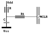
Power On Reset Algorithm The PIC16C84 crystal has a built-in power-on detector. The start timer starts counting the time delay after the supply voltage has crossed the level of about 1,2...1,8 Volts. After a delay of about 72 ms, it is considered that the voltage has reached its nominal value and another half-time delay is started to stabilize the quartz oscillator. A programmable configuration bit allows you to enable or disable the delay from the built-in start timer. The startup time varies with crystal instances, power, and temperature. See DC specifications. The generator stabilization timer counts 1024 pulses from the generator that has started to work. It is believed that the quartz oscillator has entered the mode during this time. When using RC generators, the exposure to stabilization is not performed. The external reset wait timer /MCLR is then enabled. This is necessary for those cases when it is required to synchronously put into operation several PIC controllers through a common /MCLR signal for all. If such a signal is not received, then after the time Tost an internal reset signal is generated and the controller starts running according to the program. The Tost time is programmed by the configuration bits in the EEPROM. There is a problem here where Vdd rises too slowly and all delays are at start up and the power has not yet reached its minimum Vdd(min) health value. In such cases, we recommend using external RC chains to reset to /MCLR. Below is a chain
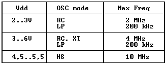
Here you can use a diode to quickly discharge the capacitor when the power is turned off. Resistor R < 40 kΩ is recommended, then no more than 0,2V will fall on it. 100 ohm resistor Watch Dog timer The watchdog timer is a completely independent built-in RC generator that does not require any external circuits. It will run even if the main oscillator is stopped, as is the case with a SLEEP instruction. The timer generates a reset signal. Generation of such resets can be disabled by writing a zero to a special WDTE configuration bit. This operation is performed at the stage of burning microcircuits. Delay WDT The nominal WDT delay is 18 ms (without the use of a divider). It depends on temperature, supply voltage, on the features of microcircuit types. If large delays are required, then a built-in divider with a division ratio of up to 1:128 can be connected to the WDT; which is programmed by writing to the OPTION register. Exposures up to 2.5 seconds can be realized here. The "CLRWDT" and "SLEEP" commands reset the WDT and the divider if it is connected to the WDT. This starts the delay from the beginning and prevents the reset signal from being generated for a while. If the reset signal from the WDT does occur, then the "TO" bit in the status register (f3) is reset at the same time. In high noise applications, the contents of the OPTION register are prone to failure. Therefore, the OPTION register must be updated at regular intervals. It should be noted that the worst combination is: Vdd=min, temperature=max and max dividing factor - this leads to the longest time delay, it can be up to several seconds. Generator types PIC16C84 crystals can work with four types of built-in oscillators. The user can program two configuration bits (FOSC1 and FOSC0) to select one of four modes: RC, LP, XT, HS. PIC16... crystals can also be clocked from external sources. An oscillator built on quartz or ceramic resonators requires a stabilization period after power-up. To do this, the built-in oscillator start timer keeps the device in the reset state for approximately 18 ms after the signal on the /MCLR chip pin reaches logic one. Thus, an external RC chain associated with /MCLR is not required in many cases. Built-in generators are operable at certain ratings of the supply voltage:
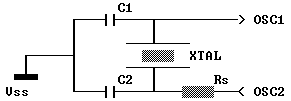
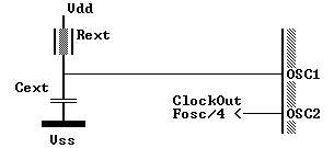
ATTENTION! At frequencies below 500 kHz, the internal oscillator may generate a faulty harmonic pulse when bit 0 of port A is toggled. This does not happen when using an external oscillator or with the built-in RC oscillator. Quartz generator PIC16C84-XT, -HS or -LP require a crystal or ceramic resonator to be connected to the OSC1 and OSC2 pins.
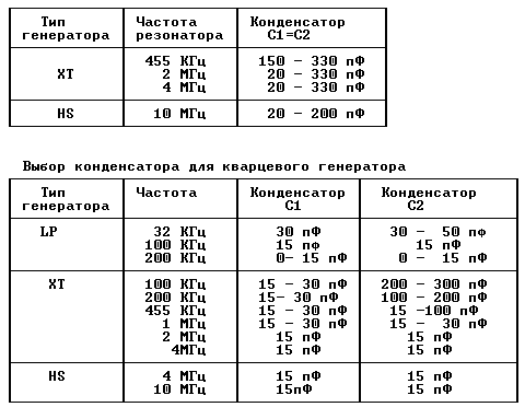
The markings are as follows: XT - standard crystal oscillator, HS - high frequency crystal oscillator, LP - low frequency oscillator for economical applications. The Rs resistor may be required for the "HS" oscillator, especially below 20 MHz to dampen harmonics. It may also be required in XT mode with an AT strip-cut resonator. The choice of capacitors for a ceramic resonator.
Higher capacitance will increase generator stability, but will also increase startup time. The values are given for guidance only. In HS and XT modes, a series resistor Rs may be required to avoid harmonics. rc generator. When speed and timing accuracy are not required, an OTP crystal such as the PIC16C84-RC saves money and implements a simple RC oscillator.
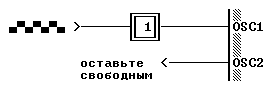
The frequency is a function of the supply voltage, resistor Rext, capacitor Cext and temperature. Also, the oscillator frequency will vary slightly from batch to batch. The generation frequency is affected by the intrinsic capacitance of the crystal case, its influence is noticeable for small values of Cext. The drift of the R and C elements must also be taken into account. For Rext values below 2.2 kΩ, the generator may be unstable or not start. At very high values of Rext (eg 1 MΩ) the generator becomes sensitive to interference, humidity and installation current leakage. The recommended Rext value is between 5 kΩ and 100 kΩ. Although the oscillator is operable without an external capacitor (Cext = 0), we recommend using a capacitance of more than 20 pF to increase stability. With little or no Cext, the oscillator frequency is highly dependent on mounting capacitances. The scatter will be the greater, the greater the value of R (and the smaller the value of C (since in this case the effect of mounting capacitances is more pronounced). The oscillator frequency divided by 4 signal is present on the OSC2/CLKOUT pin, and can be used for testing or timing purposes for other circuits. external excitation
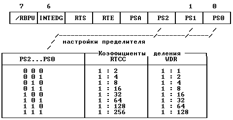
OPTION register The OPTION register (address 81h) is available for reading and writing and contains various control bits that determine the configuration of the limiter, where it is connected: to RTCC or WDT, the edge sign of the external interrupt INT and the external signal for RTCC, active load connection on the RB port. Register OPTION Address 81h Power-on value = FFH
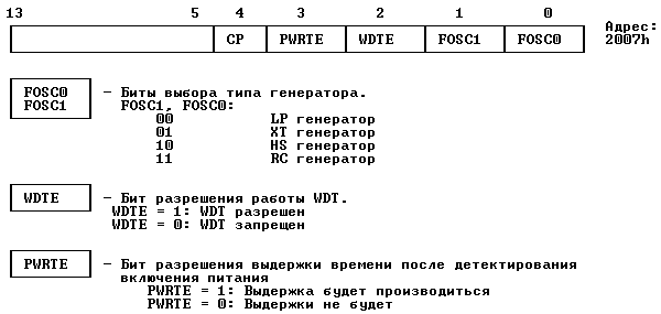
PSA - Bit connecting divider to: 0 - RTCC 1-WDT RTE - Edge of the external RTCC signal: 0 - rising edge increment on RTCC pin 1 - negative edge increment on RTCC pin RTS - Signal source for RTCC 0 - signal from the internal generator 1 - External signal on RTCC leg INTEDG - Signal edge INT: 0 - interruption on a negative edge on the INT pin 1 - positive edge interrupt on the INT pin /RBPU - Inverted active load connection bit to port B. /RBPU = 0: Active loads will be connected according to the RB port algorithm /RBPU = 1: Port B active loads are always disabled Frequency divider connections The same eight-bit counter can be enabled either before the RTCC or after the Watchdog timer. Note that the divider only works with one of these devices. We repeat, if the divider works with RTCC, it means that at the moment it does not work with the Watchdog timer and vice versa. Counter enabling scheme (see section RTCC:RTCC}. The PSA and PS0-PS2 bits in the OPTION register determine which device the divider works with and the division factor setting. When the divider is connected to RTCC, all commands that write to RTCC (for example, , CLRF 16 MOVWF 1, BSF 1,x... etc.) will reset the divider. When it is connected to the Watchdog timer, the limiter together with the Watchdog timer will reset the CLRWDT command. controllable Below is a fragment of the program for switching from RTCC to WDT 1. MOVLW B`xx0x0xxx` ;select internal clock and a new ;value for divisor. If the new value of ; divisor is 2. OPTION ;`000` or `001`, then you must temporarily select ;another divisor value. 3. CLRF 1 ; reset RTCC and divider. 4. MOVLW B`xxxx1xxx` ;select WDT without changing the divisor value. 5.OPTION 6. CLRWDT ; reset WDT and divider. 7. MOVLW B`xxxx1xxx` ;select a new value for the divisor. 8.OPTION Items 1 and 2 are only required when an external pulse source has been connected to the RTCC. Items 7 and 8 are required when the coefficient division should be set to `000` or `001`. Switching the splitter from WDT to RTCC 1. CLRWDT ; reset WDT and divider. 2. MOVLW B`xxxx0xxx` ;select RTCC, new value for divisor ;signal source. 3. OPTION These programs should be used even if WDT is disabled. Configuration word The PIC16C84 crystal has five configuration bits that are stored in EEPROM and are set during the chip programming phase. These bits can be programmed (read as `0`) or left unprogrammed (read as `1`) to select the appropriate device configuration option. These bits are located in EEPROM memory at address 2007h. The user should remember that this address is below the code area and is not available to the program. Configuration EEPROM cell.
CP - Code protection bit. CP = 1: Security code disabled CP = 0: Security code enabled The remaining bits in the word are not used and are read as ones. individual label The PIC16C84 crystal has four words located at (2000h-2003h) These are used to store the user identification code (ID), checksum or other information. Like the configuration word, they can only be read or written by the programmer. There is no program access to them. If the crystal is protected, the user is advised to use only the lower seven bits of each word ID for identification, and write `0` to the most significant bit. Then the word ID can be read even in a protected version. Protection of programs from reading Program code that is written to the chip can be read-protected by setting the protection bit (CP) in the configuration word to zero. The contents of the program cannot be read in such a way that it could be worked with. In addition, when the protection bit is set, it becomes impossible to change the program. The same applies to the contents of the EEPROM data memory. If protection is set, then the CP bit can only be erased along with the contents of the crystal. EEPROM program memory and data memory will be erased first, and lastly the CP code protection bit. Checking a crystal with protection installed. When reading a protected chip, reading any memory address will give a result similar to 0000000XXXXXXX (binary), where X is 0 or 1. To check the integrity of memory in a protected chip, follow the rules: 1) program and check the operation of a working crystal. 2) set the protection of the program code and read the contents of the program memory into the reference file. 3) Verify any protected chip by comparing its program memory with the contents of this benchmark. The EEPROM data memory cannot be checked after the security bit is set. Low Power Mode The SLEEP mode is entered by the SLEEP command. With this command, if the WDT is enabled, it is reset and starts timing, the "PD" bit in the status register (f3) is reset, the "TO" bit is set, and the internal oscillator is turned off. The I/O ports retain the state they had before entering SLEEP mode. To reduce the current consumption in this mode, the pins should be set so that no current flows between the crystal and external circuits. The input pins must be connected with external high or low resistors to avoid switching currents caused by floating high-resistance inputs. The same goes for RTCC. Leg /MCLR must be energized by Vihmc. Exit from the SLEEP mode is carried out as a result of the following events: 1. External reset - low level pulse on pin /MCLR. 2. Reset when WDT is triggered (if enabled) 3. Interrupts. (Interrupt on INT pin, interrupt on port B change, interrupt on completion of writing EEPROM data). The first event resets the entire device. The other two events suggest that the program continues to run. The "PD" bit in the status register (f3), which is set at power-up but reset by the "SLEEP" command, can be used to determine the state of the processor before "waking up": either the processor was in the "SLEEP" (warm start) mode, or it was just power off (cold start). The "TO" bit allows you to determine what caused the exit from the SLEEP mode: either an external signal on the /MCLR pin, or the operation of the WDT. For a device to wake up from SLEEP mode via an interrupt, the interrupt must be enabled by setting the appropriate mask in the INTCON register. When exiting SLEEP mode, the background program will be executed if the general mask disables all interrupts (GIE=0). If GIE=1, then the interrupt routine will be executed. Maximum values of electrical parameters Parameters outside these limits may damage the chip. Operating the crystal at its limit values for a long time will affect its reliability.
Notes: 1. Total power dissipation must not exceed 800mW for each enclosure. The dissipated power is calculated using the following formula: Pdis= Vdd(Idd - Sum(Ioh)) + Sum ((Vdd - Voh)Ioh) + Sum (Vol Iol) 2. Dropping the voltage on the /MCLR pin below Vss(ground) will induce high currents, greater than 80mA, and may damage this line. Therefore, we recommend that you apply signals to the /MCLR pin through a 50-100 ohm terminating resistor. DC parameters DC specifications: PIC16C84-04, PIC16C84-10. (For commercial, industrial, automotive performance). MEMEC BALTIC Ltd. is a member of Memec International Components Group and Raab Karcher Electronics Group. This group of distributors of electronic components is a leader in the distribution of the latest electronic technology and semiconductor components. MEMEC BALTIC Ltd. represents the MEMEC group of companies and is the official distributor of Microchip and Raychem in Russia, Ukraine, Belarus and the Baltic countries. MEMEC BALTIC Ltd. Publication: N. Bolshakov, rf.atnn.ru
Machine for thinning flowers in gardens
02.05.2024 Advanced Infrared Microscope
02.05.2024 Air trap for insects
01.05.2024
▪ Animals sense the magnetic field thanks to bacteria ▪ Wireless charging up to 30cm away ▪ Efficient cooling of 3-D chips
▪ section of the site Labor protection. Selection of articles ▪ Article Insurance business. Crib ▪ article Who was Xanthippe? Detailed answer ▪ Etna article. Nature miracle ▪ article Drilling holes with electric current. Chemical experience
Home page | Library | Articles | Website map | Site Reviews
www.diagram.com.ua |


 Leave your comment on this article: