|
|


 Arabic
 Bengali
 Chinese
 English
 French
 German
 Hebrew
 Hindi
Hindi Italian
 Japanese
 Korean
 Malay
Malay Polish
 Portuguese
 Spanish
 Turkish
 Ukrainian
 Vietnamese
|
ENCYCLOPEDIA OF RADIO ELECTRONICS AND ELECTRICAL ENGINEERING Modern TV channel selectors with frequency synthesis. Encyclopedia of radio electronics and electrical engineering
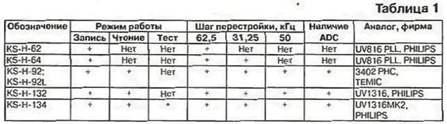
Encyclopedia of radio electronics and electrical engineering / Телевидение Selectors, the principle of which is based on frequency synthesis, are called PLL selectors ("Phase Locked Loop"). These selectors are also called digital, since they are controlled by the TV processor via a two-wire bidirectional digital I2C bus. Frequency synthesis significantly increases the accuracy of tuning to a TV station, simplifies the use of a TV, while maintaining the possibility of manual adjustment to obtain the optimal image quality [1 - 4]. Before proceeding to the description of selectors, let's clarify some terms and conventions used for PLL selectors. The flow of information on the I2C digital bus can be transmitted in two directions: from the processor and to the processor. When it is directed from the processor to a selector (for example, set commands), this mode is called WRITE. The return transmission of the information stream (from the selector) corresponds to the READ mode, which is set when the selector at some point informs the processor about its state or confirms the previously set one (at the request of the processor). Not all PLL selectors have this mode. The following notation is used: AS (Adress Select) - address bus: SDA - serial data bus; SCL (Select Clock) - synchronization bus, clock pulses; LW - synthesizer supply voltage (+5 V); ADC is a five-level ADC built into the synthesizer and allows you to control some additional device through a selector. In table. 1 - 3 shows the most important information about the PLL selectors manufactured by JSC "SELTEKA" (Kaunas, Lithuania) [5] and their analogues - available modern selectors of foreign companies (domestic models, unfortunately, have not yet been introduced into mass production) . Other general information about them and parameters were published in [1]. Recall that all of them are all-wave models of European unification. Antenna input - type IEC (SNIR), IF output - symmetrical. In table. 2 and 3 Un - tuning voltage; pin 1 is closest to the antenna input. For selectors KS-H-132. KS-H-134 has only 11 pins. In these selectors, the supply voltage is +5 V and a special output for the UPLL voltage is not provided, but there is a terminal for the tuning voltage (0,5 ... 28 V) - the UH output, which facilitates the control of the selectors and makes manual adjustment possible.
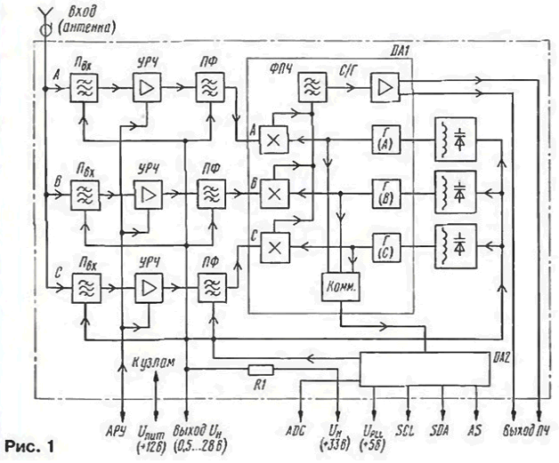
The simplest model is KS-N-62. The tuning speed, starting from a frequency of 132 MHz in sub-band A, 356 MHz in sub-band B and 678 MHz in sub-band C, changes (by software) as follows. to compensate for the non-linearity of the dependence of the capacitance of the varicaps on the tuning voltage. In the KS-H-64 selector, the tuning speed is also changed by software. The program itself is "hardwired" in the processor. KS-H-92 is a more advanced and sophisticated selector. The tuning speed is slowed down (slightly - slightly) near the TV station to reduce the residual detuning. The tables give the parameters of the upgraded (at the end of 1998) version of the KS-H-92 selector, in which the TSA5522M chip from PHILIPS is installed instead of the synthesizer from MOTOROLA. This option has become an analogue of the TEMIC selector 3402RNS. The KS-H-92L selector is a variant of the KS-H-92 with an extended antenna input (32.2 mm). The KS-H-132 selector has similar functionality, but at a low supply voltage. The newest selector to date can be called KS-H-134 (developed in 1998). It changed the boundaries of the sub-ranges of received frequencies: A - from the air channel 1 to the cable channel SK6 (47 ... 158 MHz). B - from SK7 to SK37 (158 ... 438 MHz); C - from SK38 to the 69th channel (438 ... 862 MHz). A test mode has been introduced, and the change in the speed of tuning occurs automatically. When the loop of the PLL system is closed (in the channel capture band), the tuning speed is switched, and in the absence of fixation, the reverse speed change is provided. Software enable/disable of the tuning speed function allows you to switch to manual tuning. On fig. 1 shows a block diagram of a PLL selector (using KS-H-92 as an example). It consists of three identical channels for signal extraction, amplification and conversion. Each channel is designed to operate on only one sub-band (A, B or C). Consider the construction of one of the channels, for example, for subband A.
The radio signal from the antenna input is selected by the input circuit, which acts as a bandpass filter (Pm). and passes to the radio frequency amplifier (URCh). assembled on a field effect transistor. The load of the URC is a band-pass filter (PF). The input circuit and the bandpass filter are tuned by varicaps. The amplified signal is fed to the DA1 chip, which contains three separate balanced local oscillator (S/G) mixers. The contours of the local oscillators are also rebuilt by varicaps. The IF signal is selected by a bandpass filter (PLF) and after the matching stage comes to the output terminals of the selector (IF output). The local oscillator signal through the switch (Comm) is fed to the frequency synthesizer chip DA2. On fig. Figure 2 shows a fragment of the block diagram of the synthesizer, which includes an exemplary oscillator (OG) of frequency Fo, the first programmable divider (PD1) with a division factor K and the second programmable divider (PD2) with a division factor N, a frequency-phase detector (PD) and an active filter low frequencies, which is used as an integrator (AND). The latter is not part of the microcircuit, but it works in the PLL loop and implements a change in the tuning speed. The frequency of the reference signal is stabilized by a 4 MHz quartz resonator.
The divider PD1 is designed so that its division factor K is set by the processor in strict accordance with the set tuning step according to Table. 4.
How does the synthesizer work in the ring of the PLL pulse system when the local oscillator frequency changes from Fg1 to the frequency Fg2, and Fg2>Fg1? In order for the inputs of the frequency-phase detector to have signals of the same comparison frequency (Fcp). the output frequency of the local oscillator must satisfy the ratio Fo / K = Fg / N. A change in the division factor N per unit leads to a corresponding change in the frequency F, by the minimum step of the frequency grid of the local oscillator. At the first moment after increasing N, the frequency of the signal at the output of the programmable divider PD2 will become less than Fcp and the frequency-phase detector will begin to generate corrective pulses, which are converted by the integrator into an increased control voltage (Uypr). This voltage is supplied to the local oscillator varicaps (as well as the input circuit and the bandpass filter in each selector channel). The local oscillator frequency will increase until the frequency values at both inputs of the frequency-phase detector are equal. As a result, the achieved phase difference (residual detuning) will be maintained constant. Therefore, by changing the division factor N, the frequency selector is tuned. Moreover, each value of the tuning step corresponds to a certain value of the comparison frequency (Table 4). It is easy to see that the tuning rate depends on the parameters of the integrator. Thus, an increase in the input current of the integrator by a factor of five causes a significant increase in the tuning speed. This control method is called PUMPING (Charge Pump). However, it should be borne in mind that the speed of tuning is limited by the condition of stability, as in any automatic control system. In table. 4 also gives the values of the coefficient D, necessary to determine the division factor N. To calculate its values, use the ratio N = D (Fgn + Fpch, where Fg is the local oscillator frequency for the image signal, Fpch is the image IF. In binary terms, to set the programming coefficients, the number N has the form: N=16384 N14+8192 N13+4096 N12+ 2048 N11+1024 N10+512 N9+256 N8+ 128 N7+64 N6+32 N5-4 6 N4+8 N3+ 4 N2+2.N 1+N0, where N14 - N0 are bits of information that take the value 0 or 1. And finally, we should talk about the signal exchange protocol between the PLL selector and the microprocessor control system in various modes. In the WRITE mode, the exchange protocol consists of five bytes of eight bits each: one address byte, two bytes of the PD2 software divider, and two control bytes. At the end of each byte, the selector must send a special ACK signal (Acknowledge), confirming the correctness of the received information. In general, the exchange protocol in this mode is presented in Table. 5. It should be borne in mind that the same bit in the control bytes for different selector models has different designations. For example, the P14 bit is 5I for the KS-H-62 selector, T14 for the KS-H-64, and CP for the others. Therefore, in the tables, such bits are denoted by the letter P (PORT) with a serial numerical number, and designations for a particular selector can be indicated in brackets. Bit values. marked with an X in the tables are not used for control.
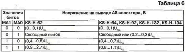
The R/W (Read/Write) address bit switches the selector to READ or WRITE mode. When R/W=0, the WRITE mode is set. For selectors without READ mode, this is the only state. MA1 and MA0 are bits for selecting the required address if the TV contains several selectors (for example, the second selector for the "Picture in Picture" device). The address change is achieved by changing the voltage at the AS pin in accordance with Table. 6. When using one selector on the TV, MA1=0 and MA0=1 or the AS output is left free.
Bits N14-N0 (see Table 5) set the division ratio of the programmable divider PD2, as already mentioned above. Bit P14, which has already been mentioned, is the pump bit. For the KS-H-62 selector, with P14(51) equal to 1, the tuning speed from certain frequencies in each subband increases. For other selectors, the same value of bit P14 (T14, CP) provides faster tuning. In the KS-H-134 selector, bits P13 - P11 (T2 - T0) control the switching on and off of the internal testing and automatic pumping modes in accordance with Table. 7.
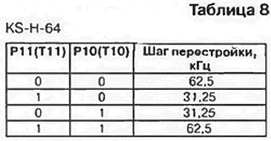
In the KS-H-64 selector, bits P11 (T11) and P10 (T10) control the programmable divider PD1 as indicated in Table. 8.
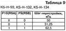
In the remaining selectors, bits P10 (RSA) and P9 (RSB) are used to control this divider according to Table. 9, and bits P13 and P12 should be 0, and bit P11 should be 1. Since the selector KS-H-62 is performed with a single tuning step (62,5 kHz), then for it, bits P11, P10 and P9 are equal to 1. Bit P8 is 0 for all selectors without exception.
The subband switching is concentrated in the last control byte. Moreover, the number of bits used can be from three to five (the remaining bits are not used). For the KS-H-62 selector, this is P7 - P10 in the table. 64, for KS-H-0 - РЗ (ВЗ) - Р0 (В11) in the table. eleven.
For KS-H-134 (Table 12), KS-H-92 and KS-H-132 (Table 13) use the three least significant bits of P2 (BS2) - P0 (BS0).
In READ mode, the exchange protocol consists of an address byte and a status byte. The R/w bit in the address byte must be equal to 1. There are no other changes in this byte (see Tables 5, 14).
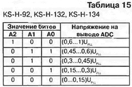
Status byte for KS-H-92 selectors. KS-H-132. KS-H-134 is presented in table. 14. The POR (Power On Reset) bit signals that the selector is powered on. The POR bit is 1 when power is on. Bit FL (In lock Flag) - a signal about the action of the PLL system. When the FL bit is 1, the PLL ring is closed. The ACPS (Automatic Charge Pump Switch flag) bit informs about the operation of the automatic PUMP switching device in the KS-H-134 selector. The ACPS bit is active in state 0. Bits A0-A2 are the output signals of the five-step ADC (ADC). For selectors with the READING mode (see Table 14), the ADC parameters and combinations of A0-A2 levels are the same and are shown in Table. 15. ADC allows, for example, to control a selector via a three-wire bus (American standard).
A few more words about control processors. There are quite a few of them. They differ from one another by filling the internal ROM ("firmware"). For selectors KS-H-92. The KS-H-132 is best suited for the PCA84C640-30 processor from PHIUPS. Literature
Author: A.Burkovsky, St. Petersburg
Alcohol content of warm beer
07.05.2024 Major risk factor for gambling addiction
07.05.2024 Traffic noise delays the growth of chicks
06.05.2024
▪ Created a liquid with a negative mass ▪ The desire to hug is in women's genes. ▪ Keychron Q1 HE Wireless Keyboard ▪ Industrialization has changed the planet's climate
▪ section of the website Basics of First Medical Aid (BFA). Selection of articles ▪ article Where is it seen, where is it heard? Popular expression ▪ article What was in America before its discovery by Columbus? Detailed answer ▪ article driver of the vehicle. Job description ▪ Article Wonderful thread. Chemical experience
Home page | Library | Articles | Website map | Site Reviews
www.diagram.com.ua |


 Leave your comment on this article: