|
|


 Arabic
 Bengali
 Chinese
 English
 French
 German
 Hebrew
 Hindi
Hindi Italian
 Japanese
 Korean
 Malay
Malay Polish
 Portuguese
 Spanish
 Turkish
 Ukrainian
 Vietnamese
|
ENCYCLOPEDIA OF RADIO ELECTRONICS AND ELECTRICAL ENGINEERING Chip TDA8362 in 3USCT and other TVs. Encyclopedia of radio electronics and electrical engineering
Encyclopedia of radio electronics and electrical engineering / Телевидение Many families still operate obsolete TVs - ULCT, UPIMCT and even 3USCT. Their owners, having experience in amateur radio design, would like to endow their devices with a number of features inherent in new modern models, improve the quality of the received image and some parameters. This article explains how you can upgrade old TVs using the TDA8362 chip. Mass production of color televisions in our country began in 1973 with the release of a unified lamp-semiconductor model ULPCT and later - ULPCT (I), which were replaced by the UPIMCT series and later - 2USCT and 3USCT. Their annual output in the best years exceeded two million pieces. Even though in 1991 fourth-generation devices appeared, the bulk of production until recent years was 3USCT televisions. It is not surprising that after the collapse of the USSR, the inhabitants of Russia left more than 40 million color television sets, mostly of the first or third generation. All of them, from the point of view of the modern user, are considered obsolete both morally and physically. If the question of the obsolescence of devices is clear, then their physical aging can be judged if we recall that the age of the ULPCT TVs preserved by the population reaches 20 ... 25 years (their production was discontinued in 1978). There are 15-20 million televisions of the UPIMCT (5-6 years old). According to pre-existing norms, the service life of the TV set was 3 years. From this point of view, all the devices ULPCT, UPIMCT and part of the 20USCT have already served their purpose and should seem to give way to new ones. However, articles with proposals for the modernization of old TVs still appear in the Radio magazine and in other literature. And this is good. It is possible and necessary to think about prolonging their life. This is also necessary because the financial situation of many families does not allow them to replace their existing TV with a new one. In addition, at least 10-15 million 3USCT devices have not worked out their due date and can still serve their owners. All this allows us to consider that the problem of modernizing TVs in order to extend the service life, increase reliability and introduce new functions, subject to low costs (no more than 20% of the cost of a new device) is very relevant and remains so for more than one year. One of the ways to solve this problem is the introduction of a modern element base into obsolete TVs. But before moving on to specific proposals, let's look at a little history. Integrated circuits in domestic televisions were first used in 1976. in one of the ULPCT(I) models, in which the BCI color module was used on K224 series microcircuits. Wider use of the microcircuit was found two years later in TVs UPIMTST, when the electronics industry began mass production of the K174 series. Its first devices had a low degree of integration and needed a large number of external radio components. So, ten ten microcircuits in the signal processing unit (BOS) of the UPIMTST TV were accompanied by 440 different parts. By modern standards, this is too much for a radio channel and a color channel. The table published here contains information about the number of parts in the blocks of the radio channel, synchronization, color and output video amplifiers of TVs of different generations. It follows from it that the situation improved slightly with the advent of 2USCT and 3USCT TVs, in which more advanced K174 series microcircuits were used.
However, the number of attachments was still large, which reduced the operational reliability of these most popular TVs. Reliability was also reduced by a large number of adjustment elements for adjustment during production and after repair, and the presence of two dozen pairs of interblock connectors with a hundred contacts. It is no coincidence that TV sets of the fifth or sixth generations clearly showed a trend towards the use of highly integrated microcircuits, which, while expanding the list of functions, preserve or even reduce both their number and the composition of the outer frame, and reduce the number of adjustment elements (points). Numerous connectors are now being eliminated, abandoning the cassette-modular design and returning to the monoblock chassis - the basis of the first industrial and amateur televisions. Where it is impossible to refuse connectors, their new, more reliable models are used. As for microcircuits, in TVs of the fourth or fifth generations, the radio channel and color paths still contain five or six cases and require the same number of attachments as the third generation models. Against this background, multifunctional microcircuits from Philips stand out for the better, allowing sixth-generation TVs to solve circuitry problems more economically and implement a radio path and a color path on three cases while reducing the outer frame by half. These include LSI TDA8362, TDA8375, TDA8396, of which the first is most widely used. It is used not only by leading foreign companies (for example, Panasonic-TX-21S TV, etc.), but also in the CIS ("Horizon-CTV-655", "Electron-TK-570/571", "TVT-2594/2894 "). In some models, not three, but six microcircuits are used, which is explained by the use of integrated video amplifiers that dissipate less power and reduce the number of transistors from 14 to 3. Of course, the TDA8362 chip can also be used in TVs of outdated models when they are upgraded (replacing the radio channel, color and synchronization blocks with more advanced ones). A detailed description of the structure and operating parameters of the TDA8362 chip is given in [1] and [4]. It provides processing of black-and-white and color television signals both at intermediate frequency (IF) and given in the form of color difference and color signals encoded according to SECAM, PAL, NTSC systems. In this case, the IF signals can have, as usual, the negative modulation used, and the positive modulation used in the French standard L. Video signals can be presented in VHS and S-VHS formats. It also processes M (4.5 MHz), B, G, H (5.5 MHz), I (5.996 MHz), D, K, L (6.5 MHz) FM audio and AF audio signals, as well as horizontal and vertical synchronization (the latter at frequencies of 50 and 60 Hz) with the number of lines per frame within 488...722. The implementation of all these functions in one microcircuit is achieved using conventional bipolar transistors for processing analog signals of any frequency and transistors of the MOS structure for solving problems by digital methods. There are several modifications of the microcircuit, differing in the list of implemented functions and pinout. In full, all these functions are provided in the TDA8362A, but the TDA8362 and TDA8362N3 modifications are much cheaper, although they have insignificant differences. An analysis of the capabilities of the TDA8362 chip shows that their use in full in our conditions is not required. Many will consider the ability to process NTSC signals to be superfluous, since on-air programs encoded according to the NTSC-M-3.58 system are not available to our viewers (with the exception of those living in Chukotka and southern Sakhalin). NTSC-4.43 signal processing may only be needed when viewing recordings on video cassettes and video discs made in the USA, Japan and Korea. Of course, it is not required to receive signals in the H, I standards and signals with positive modulation of the SECAM-L standard. However, work according to the specified standards (H, I, SECAM-L, NTSC-4.43) is already provided for in the TDA8362 chip and you cannot refuse them, you can only not use them. Probably, from the above considerations, in [2] a typical scheme for switching on the TDA8362A modification for processing only signals from SECAM, PAL systems and standards B, G, D, K is considered. In accordance with them, a radio channel, color and synchronization module (MRCC) is offered to radio amateurs on TDA8362 chip, adapted for use in a 3USCT TV of any modification. Recommendations will also be given for those who wish to introduce the ability to receive signals from the NTSC-4.43 system into the module and use the module in other types of TVs. The MRCC module replaces the radio channel (A3) and color (A1) modules with the submodules SMRK (A2), USR (A1.3), SMC (1.4) in 2.1USCT TVs. The cassette-modular design of the chassis of 3USCT TVs simplifies the work of replacing modules, reducing it to removing two boards and installing a new one in their place. The module is powered by 12 and 220V voltage sources available in the TV. The current consumption in the 12V circuit is 160mA (instead of more than 500mA for replaceable modules), which has a beneficial effect on the operation of the rectifier in the TV power module and reduces power consumption. Consider the circuit diagram of the module, starting with its radio path. It includes channel selectors, preamplifier with SAW filter, UPCH, IF demodulator, APCG and AGC devices. A block diagram showing the relationship of these blocks is shown in Fig.1.
Figure 2 shows a schematic diagram of the path. Depending on the type of program selection device (UVP), the diagram shows options for connecting the USU-1-15 (SVP-4/5/6) blocks and the MSN-501 synthesizer (drawn with thick lines).
The sensitivity of the TDA8362 chip (DA1 in Fig. 2) at the input (pins 45 and 46) is 100 μV, and according to existing standards, the sensitivity of the TV in subbands I, II should be no worse than 40 μV at the antenna input. Therefore, the transfer coefficient (gain) Ku in the circuit from the antenna input to the microcircuit input must be at least 8 dB. The circuit contains a channel selector SK-M-24 (Ky=15 dB) and a SAW filter ZQ1 (Ky < -25 dB). This means that when the selector is connected directly to the filter, the input sensitivity of the TV will be below the norm by at least 18 dB (approximately 320 μV), which is unacceptable. To preserve it, a pre-amplifier based on the VT1 transistor with Ku > 20 dB is included, which allows to compensate for the attenuation in the ZQ1 filter with a small margin. We note in passing that the Ku of the modern all-wave selector UV-917 from Philips is at least 38 dB at a very low noise level, which allows you to directly connect it to the SAW filter and at the same time provide twice the sensitivity of the TV. Such a selector is used in the TV set "Horizon - CTV-655". The ZQ1 band-pass filter must meet the following requirements: operate on an IF image carrier of 38 MHz, have a wide horizontal frequency response section ("shelf") in the 31.5 ... 32.5 MHz band and a balanced output. These requirements are met by surfactant filters KFPA-1007, KFPA-2992, KFPA-1040A. The widely used filters KFPA-1008, K04FE001 have a narrow "shelf" and will not provide reception according to standards B, G. The FPZP9-451 filter used in 3USTST TVs has an unbalanced output, which requires the introduction of a balancing cascade between it and the microcircuit on two transistors. After amplification in the UPCH (see Fig. 1), the IF signals in the demodulator are converted into a full color television video signal (PCTV). The demodulator contains a white spot inversion node (limiting PDTV emissions caused by interference) at a medium brightness level, which improves image quality, preventing the appearance of noise on the screen, as well as a sharp change in the amplitude of the PDTV and the sync pulses included in it. The oscillating circuit L3C18 (see Fig. 2) serves as a common reference circuit for the IF demodulators and the APCG device, which reduces the number of tuning elements in the module. The voltage of the APCG (UAPCG) at the control point X1N during signal capture can vary within 0.5 ... When using UVP of the USU, SVP type, the voltage UAPCG is supplied to the selectors through the R12R13R18C10R7C11 circuit, where it, adding up with the presetting voltage UPN coming from the UVP through resistor R8, forms the selector tuning voltage UN. In the case of using the voltage synthesizer MSN-501, the addition of voltages UAPCG with UPN and the formation of UН occurs in the synthesizer. The voltage UAPCG is applied to it through the circuit R12R13R105C23, and the resulting value UH passes to the seoectors from pin 6 of connector X2 (A13) through the circuit R8C11R7C10. Let's return to the exemplary circuit L3C18. Each TV is characterized by such a feature: in the process of pre-tuning to some program with the APCG device turned off, it turns out that the capture bandwidth of the image carrier when approaching it from the low frequencies is wider than the same band when tuning from higher frequencies. This phenomenon does not arise from poor adjustment of the APCG. It is explained by the fact that the image carrier, with the correct setting of the selectors, is located on the slope of the frequency response of the band-pass IF filter (it doesn’t matter if it is a SAW filter in 3USCT TVs or a lumped selection filter in UPIMCT). The slope of the frequency response leads to the asymmetry of the signal applied to the demodulator of the AFCG device, which is especially noticeable at a weak input signal, when the noise level, which is smooth at the input of the channel selector, becomes noticeably asymmetric at the input of the AFCG system. As a result, there is a voltage shift UAPCG from the correct value, which causes the detuning of the receiver and the specified asymmetry of the capture band. When using the TD8362 chip, measures were taken to eliminate such a defect by turning on the C19R19 circuit. The voltage UARU is applied to the channel selectors from pin 47 of the microcircuit through the circuit C13R11C12R10R9. Its initial level is set by a tuning resistor R15. From pin 4 of the chip, pin 2 of connector X10 (A13) receives the synchronization identification signal (SOC) used in the voltage synthesizer to control the automatic program tuning system. The signal voltage UCOS is zero if there are no synchronization pulses at the input of the microcircuit. The voltage UCOS is equal to 6 V if the signal of the NTSC-3.58 system comes to the input, or * V if the "color" or "black and white" signal of the SECAM, PAL, NTSC-4.43 systems is received. From pin 7 of the PDTV microcircuit, it enters a set of external filters, where it is divided into a video signal and an FM audio signal. Bandpass filters ZQ2, ZQ3 select frequency bands in which FM audio signals are placed (5.5 +/- 0.05 MHz in B, G standards and 6.5 +/- 0.05 MHz in D, K standards). Through pin 5 of the microcircuit, as shown in Fig. 3, they pass to the demodulator, and then to the audio input switch. The FM audio demodulator has a phase-locked loop (PLL) system that provides automatic tuning to any audio standard. Notch filters ZQ4, ZQ5 (see Fig. 2), clearing the PDTV from the bands occupied by FM audio signals, turn it into a video signal, which is fed through pin 13 of the microcircuit to the video input switch (see Fig. 3). Figure 3 also shows the switch R, G, B, we will consider its operation further.
Audio and video input switches also receive signals from external sources (VCR, video disc player, video game console). The control of the switches (AV/TV function) is ensured by applying the appropriate voltage to pin 16 of the microcircuit: less than 0.5 V to turn on the on-air program (TV); 3.5...5 V to turn on an external program in S-VHS (AV) format; 7.5...8 V for operation from an external source of VHS (AV) format. If there is no voltage at pin 16, the chip operates in TV mode. Recall that the recently appeared S-VHS video recorders (for example, Philips-VR969) provide higher image quality (400-430 lines versus 230-270 lines for VHS video recorders and 320 ... 360 lines for on-air programs). This is achieved by placing the color component not in the usual 3...4,7 MHz PDTV band, but in the 5.4...7 MHz band. During playback, such video recorders are connected in three circuits: the audio signal is connected to pin 6 of the microcircuit, the brightness signal S-VHS-Y is connected to pin 15, the color signal S-VHS-C is connected to pin 16. If there is only one external source of video signals in VHS format, then it is connected to the MRCC as shown in Fig.4.
When using the MCH synthesizer, the AV/TV signal comes from it through connector X7 (A13). If USU, SVP blocks are used, then you will have to manually receive the AV / TV signal with the SA1 switch in two positions, installed in a convenient place on the TV case. In both cases, in TV mode, a voltage of no more than 0.4 V is generated (or it is absent), and in AV mode, at least 10 V. The latter is transmitted to pin 16 of the microcircuit through a switch on the VT4 transistor. The type of input and output connectors XS1, XS2 is selected depending on the type of their counterparts in the signal source used. If there are several sources of video signals, then they are connected to the MRCC through a matching device. Detailed information on its construction is given in [3]. The MRCC video path is assembled on six microcircuits: TDA8362, TDA8395, TDA4661 and three TDA6101Q. It includes a rejection node, signal demodulators of various broadcasting systems, a delay line, a matrix, an R, G, B input switch, an OSD device, and video amplifiers. The relationship of these devices is shown in Fig.5. In the video path, the video signal is converted into color difference and then into color signals.
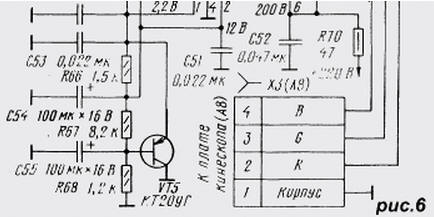
A feature of the TDA8362 microcircuit is the construction of notch and bandpass filters of the color path (flare filter, etc.) without external coils, while in the MTs-2/3/31 3USCT TVs, six or seven adjustable oscillatory circuits are used for this. If you do not take into account video amplifiers, then in the video path there are no elements at all to be configured. The rejection unit cuts out the color component C from the video signal - the frequency band occupied by the subcarriers of the color difference signals. Recall that in the NTSC system the subcarrier frequency is 3.58 MHz, in the PAL system it is 4.43 MHz. In the SECAM system, there are two subcarriers with frequencies of 4.25 and 4.406 MHz. Frequency determination, depending on the broadcasting system, occurs automatically in the node. Rejection depth - 20 dB, which provides effective cleaning of the luminance signal from the chrominance subcarriers with a minimum width of the cut out bandwidth. This enhances the clarity of the image. When a black-and-white image signal is received, the rejection unit recognizes it and turns off. The luminance Y component passes into the synchronization path and into the matrix. The color component is fed to the demodulators. The demodulator of PAL, NTSC signals is located in the DA1 chip. As a result of its work, color difference signals RY, BY are distinguished, which, through pins 30 and 31 of the microcircuit, come to the signal delay line by one line (DA3 microcircuit). In it, NTSC signals are filtered, and PAL signals are averaged over two lines following one after the other. From the output of the DA3 chip (pins 12 and 11), the processed signals RY, BY of the PAL and NTSC systems are again returned to the DA1 chip through pins 28 and 29. The SECAM signal demodulator is contained in the DA2 chip. Through pin 27 of the DA1 chip, component C of the SECAM system is fed to the DA2 chip, and from pin 32 of the DA1 chip, a signal with a frequency of 4.43 MHz, necessary for the operation of the demodulator, is supplied. The received color difference signals RY, BY of the SECAM system from pins 9 and 10 of the DA3 chip also pass to the delay line, where the correct sequence of direct and delayed lines is formed in each of the color difference signals. The signals RY, BY coming from the DA3 chip of all systems in the DA1 chip, after equalizing the time delays, enter the matrix, where, mixing with the brightness component Y, they are converted into color signals R, G, B. Through pins 22-24 of the DA1 chip, signals come to the switch R, G, B from an external source - a computer (see Fig. 3 and 4). The control of the switch is provided by the voltage of the blanking signal FB ("Window") supplied from the computer to output 21. If it is absent, signals from the matrix pass to the switch output, and if FB<5 V - from the computer. Then the signals R, G, B come to the output video amplifiers. Video amplifiers (VU) are high-voltage powerful operational amplifiers TDA6101Q. Their main advantage is broadband and the absence of powerful resistors in the output circuits (no more than 0.5 W). They have sensors of the automatic white balance system (ABB), but since the TDA8362 chip (unlike other modifications) does not contain the means to control the ABB system, this function is not used. Let's consider the operation of the VU (Fig. 6) using the example of the passage of signal B. From the output 18 of the DA1 microcircuit to the input of the op-amp (pin 3) DA6, the signal B enters through the divider R60-R63. Resistor R62 "Black Level B" sets the constant component of the output signal equal to 125 V. Resistor R61 "Peak B" aligns the variable component of the signal B with the same value of the signal R. Resistor R63 is used when adjusting the white balance "in black" (at the blanking level kinescope rays), and resistor R61 - when adjusting the white balance "in light" (at the level of normal brightness).
At the point of connection of resistors R60, R61 with MSN comes component B of the signal for displaying information on the screen (OSD system). At the connection point of resistors R61, R63, a deep negative feedback signal passes through resistor R64 from pin 9 of the DA6 chip. Resistor R65 protects the video amplifier from discharges occurring in the kinescope. Capacitor C49 corrects the frequency response of the amplifier at high frequencies. Capacitors C51 and C52 - filtering in the supply voltage circuits +12 and +220 V. Capacitor C50 - filtering in the circuit of the reference voltage +2.2 V, necessary to stabilize the operation of the amplifiers. It is formed by a stabilizer on the transistor VT5. The X8N control points are necessary when adjusting the purity of color and convergence of the kinescope beams. When they are closed, beam B is extinguished. Point X11N serves to check the level and shape of the signal supplied to the kinescope. Video signal amplifiers R and G are built similarly, except that there is no peak-to-peak regulator in the R path. The circuits for connecting the adjustments of the image and sound parameters to the MRCC are shown in Fig. 7.
Volume control in 3USTST is provided by changing the resistance of the resistor circuit R206, R207 in the control unit (A9), connected between the UPCHZ-1/2 microassembly in the MRK module and the common wire. When using the TDA8362 microcircuit, the adjustment occurs when the voltage at its pin 5 changes within 0.1 ... 3.9 V. To do this, if there is a SVP or USU, the R80C60R78 circuit is connected together with resistors R207, R206 in the control unit. Resistor R207 (it is designated as R33 in BU-3 / 3-1, R7 in BU-4, R6 in BU-5 and R15 in BU-14) must have a resistance of 1 kOhm. When using the MCH, the volume control circuit includes elements R80, C60 and a resistor R34 in the MCH. In this case, in the MSN, the VD5 diode is closed with a jumper, and the resistance of the resistors R28, R29 should be 18 kOhm. Brightness, contrast and saturation when using SVP and USU are still regulated by variable resistors R201, R203, R205 located on the front panel of the TV. Since the regulating voltage is removed from their engines in the range of 0 ... 12 V, and a signal of no higher than 1 V must be applied to the DA5 chip, voltage dividers R5R9, R72R73, R74R77 are connected after the contacts of the X75 (A76) socket. When using the MCH, all adjustments are made through the module from the remote control or from the keyboard on the front of the TV. All TV control resistors will be turned off. In both cases (when using SVP, USU or MSN), the control voltages of the adjustments are transmitted to pins 17, 25, 26 of the microcircuit through circuits that include filter capacitors C57-C59. When using SVP, USU, they stabilize the control voltage, and when working with the MSN, they average the pulse signals of variable duty cycle adjustments generated by the module. Through the elements VD8, R71, C56, the contrast control circuit is supplied with a beam current limiting voltage (ECL), which reduces the amplitude of the R, G, B signals entering the WU, with an increase in the total beam current above the norm. At any UVP, the color tone adjustment resistors are disabled. The synchronization path consists of horizontal and vertical sync selectors, horizontal scanning trigger generators (SIzap) and vertical scanning pulses. The horizontal sync selector separates the horizontal sync pulses from the luminance Y component of the video signal coming from the video input switch. The Y signal, the amplitude stabilization of which was provided in the radio path by an effective AGC and a white spot inversion unit, is limited by the maximum and minimum so that the horizontal and vertical blanking signals, as well as the "flashes" of the color synchronization signal, are guaranteed to be cut out at any range of the Y brightness component. The cleared horizontal sync pulses of stable amplitude are fed to the first loop of the PLL system, which corrects the frequency of the SIzap pulses according to them. The sync capture bandwidth of the first loop is +/-900 Hz, and the captured sync retention bandwidth is +/-1200 Hz, which is significantly better than the corresponding indicators (+/-700 Hz) for the K174XA11 chip used in the USR submodule of 3USCT TVs. The second loop of the horizontal PLL, as usual, ensures the stability of the position of the left vertical border of the image. Resistor R91 "Phase" (Fig. 8) allows you to correctly set the phase of the image. SIzap pulses with an amplitude of 0.8 V from pin 37 of the DA1 microcircuit pass through the emitter follower on the VT7 transistor to pin 2 of connector X5 (A3) and then to the line scan module.
Vertical scan control pulses are formed in the DA1 chip from a sequence of pulses SIzap by dividing it by the number of lines in a half-frame of the image (determined in the process of identifying the coding system for color signals) with the correction of the origin of the frame sync pulses (FSI) coming from the frame sync selector. Such a construction facilitates the search for vertical sync pulses in a wide band (45 ... 64.5 Hz). As soon as 50 sequentially received frame sync pulses (FSI) are within the wide capture band, the system switches to a narrow band in which it will continue to work. If six consecutive KSI go beyond the narrow band, the device enters the mode of searching for them in a wide band. Vertical sweep sawtooth pulses (CST) with an amplitude of 1.25 ... 1.5 V are formed at pin 42 of the DA1 microcircuit by an integrating circuit R92C67, to which a +31 V voltage is applied, stabilized by a VD11 zener diode. The linearity of the pulses is improved by applying a personnel negative feedback (OOS) voltage with an amplitude of 1 V, which comes to pin 41 of the DA1 chip from the OOS sensor - a resistor included in the personnel deflecting coil circuit. In addition to improving the linearity of the CPT, the CNF sensor performs the function of monitoring the operation of the vertical scanning output stage. If the voltage on it is less than 1 V (an open in the chain of frame coils) or more than 4 V (the output stage is faulty), the outputs R, G, B of the DA1 chip are closed to avoid burning the kinescope. In 3USCT TVs, the frame signal is generated in the frame scan module MK-1-1 on resistor R27. In the PSP board (A3) it is available on pin 2 of connector X1 (A6) and on pin 11 of connector X3 (A7). To transfer it to the MRCC, you can use the SIstrob circuit released with the introduction of the module, connecting pin 10 of connector X5 (A1) and pins 4 of connectors X4 (A2) and XN1 on the PSP. All these circuits are shown in Figure 9. To implement the proposal, connect pin 11 of connector X3 (A7) and pin 4 of connector XN1 on the PSP with a jumper. Figure 9 shows a view of the board from the side of the printed conductors. The dashed line shows the jumpers located on the side of the sockets.
In televisions with a TDA8362 chip, the TDA3651 / 54 (K1021XA8) or TDA3651Q / 54Q (K1051XA1) microcircuit, which has current control, is usually used in the vertical scan output stage. The frame trigger pulse transmitted from pin 43 of the TDA8362 chip to such an output stage is a current pulse with an amplitude of at least 1 mA during the forward path of the beam and several microamperes during the reverse stroke. It corresponds to the voltage at pin 43 with a level of 5 V for forward and 0.3 V for reverse, i.e. short retrace trigger pulses are directed downwards from the 5 V level. In 3USTST TVs, the control of the MK-1-1 module is provided by positive (upward-directed) vertical scanning trigger pulses with an amplitude of 10 V. An amplifier is used to match the shape and amplitude of the pulses coming from pin 43 of the DA1 microcircuit with those required for the MK-1-1 module. inverter assembled on a transistor VT6 (Fig. 8). The connection diagram of the MRCC with the rest of the 3USST TV units is shown in Fig. 10.
Before proceeding to the description of the module design, let's consider its possible modifications depending on the type of TV being upgraded and the wishes of its owner. 1. Channel selectors SK-M-24-2 and SK-D-24 will work successfully in MRCC, however, replacing them with more modern all-wave selectors SK-B-618, KS-V-73 and especially UV-917 will significantly increase the sensitivity TV, improve the signal-to-noise ratio and simplify the module due to the direct (without transistor VT1) connection of the selector with the filter ZQ1 (see Fig. 2). The presence of a combined antenna input for these selectors for MV and UHF eliminates the problem of connecting to the two antenna inputs of the 3USST TV of the distribution network of the collective reception. 2. The list of color television systems processed by the TDA8362 chip is determined by the voltage at its pin 27. If it is more than +5 V (pin 27 is connected to the +44 V voltage conductor through resistor R8, as shown in Fig. 6), then only signals are processed SECAM and PAL systems. If there is a need to process any of the NTSC systems, then the circuit for connecting output 27 of the microcircuit should be mounted in accordance with Fig. 11 by installing elements R102-R104, C78, VD12 and removing resistor R44.
When using UVP types USU, SVP, the NTSC color tone control (in this system such an operational adjustment is necessary, since a change in the amplitude of the brightness signals causes a change in image color) is a variable resistor R211 (Fig. 11) - one of the two color tone controls installed on the case TV. When setting the MCH to adjust the NTSC color tone, the adjustment that is not used in the standard inclusion of the synthesizer is used, which is output to pin 6 of the D2 MCH chip. To do this, pin 6 of the D2 chip is connected to pin 9 of the X10 MCH connector through a 104 kΩ resistor R20. The TONE symbol will appear on the screen as an indication of the adjustment. If you wish, the designation can be replaced with the correct HUE (color) if you turn on the VD11 diode between pins 20 and 38 of the D2 MCH chip, unsoldering pin 38 from the common wire. All this will allow you to receive NTSC-4.43 signals from the video input. As for the signals of the NTSC-3.58 system received from the antenna input, their processing requires a serious change in the radio path. It is necessary to include in it a band-pass and notch filters at a frequency of 4.5 MHz. Parallel connection of three notch filters between the transistor VT2 and pin 13 of the DA1 chip (see Fig. 2) will result in a too wide frequency band being cut out in the video signal, which will degrade the image clarity. To solve this problem, PANASONIC TVs based on the MX3C chassis [4] use a special microcircuit that recognizes the standard and includes only one required notch filter. Its addition would significantly complicate the MRCC, and therefore is not recommended. 3. The same modules are used in the 2USCT TV as in 3USCT. The pinouts of all connectors are the same, and the installation of MRCC in these TVs does not cause additional problems. 4. This is not the case with the 4USCT series. Before manufacturing a module for them, it is necessary to compare the pinout of the module connectors with the pinout of the mating parts of the TV and make the necessary changes to the MRCC. The dimensions of the module board given below correspond to the dimensions of the 3USCT cassette and may not match the dimensions of the chassis of the TV being upgraded. it may be necessary to re-layout the MRCC board. It is impossible to give more specific recommendations, since, unlike 3USCT, the circuit diagrams and printed circuit boards of 4USCT TVs from different factories are not unified and differ greatly from each other. It is proposed to be guided by the factory scheme of the modernized TV and the reference book [5]. 5. In the TV UPIMTST, the MRCC module may well be used to replace the BOS signal processing unit, provided it is supplemented with the UM1-3 (UZCH) module and the kinescope beam damping cascade (both are on the BOS). Another (in relation to 3USTST) size of the cassette requires an increase in the size of the board without changing the pattern of printed conductors. With the simultaneous replacement of the SK-V-1 selector (Ku which is lower than that of the SK-M-24-2) with a more modern one, and the UVP of the SVP-4 type with the MSN in the UPIMTST, you can get all the functions of a fifth-generation TV. 6. In the transition from UPIMCT to 3USCT model 3USCT-P (it is also 4UPIMCT), the MRCC module could replace the entire BROS scanner and signal processing board, on which the radio channel, brightness and color channels are located. It has a selector SK-M-24, modules UM1-1, UM1-2, UM1-3, UM1-4, UM2-1-1, UM2-2-1, UM2-3-1, UM2-4-1 , M2-5-1. All of them, except for the selector and UM1-3, are not needed. The M3-1-1 synchronization module installed on the BROS scan board is also not needed. Replacing this set of modules with a new one (MRCC) is, of course, possible and desirable, but it requires serious alterations in the module and the remaining BROS board due to a completely different system of interboard connections and is not recommended. 7. Installing the MRCC in ULPCT TVs is quite simple: you need to remove the DBK and BC blocks and place the MRCC instead of the BRK, making small changes in other blocks. Such a replacement leads to a very effective result - two of the three most bulky TV blocks are eliminated, power consumption is significantly reduced, and the number of radio tubes is more than halved. All this significantly improves the temperature regime in the TV case - its "Achilles heel", the main cause of frequent fires. Instead of the connectors indicated in the previously considered diagrams, a Sh15 socket is installed on the MRCC board and cables are connected to the Sh2a, Sh7a, Sh15a plugs to supply the necessary voltages and signals. The Sh9 cable connecting the DBK with the BC is removed as unnecessary. Instead of a tube ultrasonic frequency converter, the UM1-3 module from UPIMCT should be used. The SK-M-15 drum selector used in the TV, which has a very low gain Ku (8 dB), is replaced by SK-M-24, SK-D-24 or a more modern one with a UVP type USU-1-15 or MSN -501. A significant reduction in the current consumption for all supply voltages requires the selection of the values of the quenching resistors in the collector unit in order to return to the standard nominal voltages. The +12 V voltage in the ULPCT is formed in the control unit from the +24 V voltage with a stabilizer from a quenching resistor and a D814B zener diode. This node is too weak to power the MRCC and must be replaced with a unit designed for a higher current. If the owner of the TV being upgraded satisfies the previously accepted module parameters - accept only SECAM and PAL systems, B and G standards in the 3USCT TV with selectors SK-M-24-2, SK-D-24 - then you can assemble the MRCC without any changes according to the concepts previously discussed. The printed circuit board of the module is shown in fig. 12, a and b. It is suitable for any type of UVP with the following caveat. When using MCH-501, all printed conductors shown in fig. 12, a and b with solid and dashed lines, as well as all the details, except for the resistor R78.
When using UVP types USU, SVP, printed conductors shown by dashed lines are not made, and parts VD1, VD5-VD7, R35, R81-R84, C23, X7 connector (A13) are not installed. Connector X10 (A13) is replaced by X5 (A9). The changes that must be made on the printed circuit board are shown in Fig. 13, a: resistors R46, R47, R79 and capacitor C40 are placed in the same way as in fig. 12, a. Capacitors C57-C59 are placed in a new way, together with resistors R72-77.
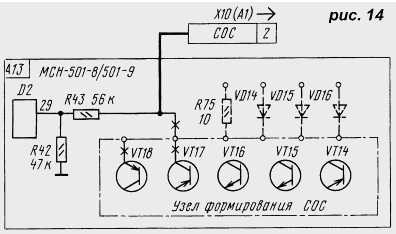
Connector X2 (A13) is replaced by connector X2 (A10). At the same time, its contacts 2, 3, 5, 6 are switched on in the same way as contacts 3-6 of connector X2 (A13), as shown in fig. 13b. If you want to use any of the modifications listed above, it is useful to draw up a complete schematic diagram of the future module based on the previously considered diagrams and recommendations, selecting the necessary elements from them. Then make the necessary changes to the printed circuit board of the module (in the pattern of printed conductors). Module parts are placed on a board made of double-sided foil fiberglass 2 mm thick. The tracing of the printed conductors of the module is made taking into account the placement of the leads of the parts in the nodes of the grid 2,5 (2,5 mm) and the reduced distance between the pins of the TDA8362 chip (1,778 instead of the usual 2,5 mm). This forced the latter to be output to both sides of the board. In the detailed description microcircuit TDA8362 [1], which you should get acquainted with, the need for tracing the board to ensure the minimum length of conductors between terminals 28, 29 of the TDA8362 microcircuit and terminals 11, 12 of the TDA4661 microcircuit, as well as from the common wire (pin 9 of the TDA8362 microcircuit) to the capacitors, connected to its pins 12, 33, 42. Pin 3 of the TDA4661 chip (the common wire of its digital part) and the pin of the capacitor C32, connected to a common wire, with a separate conductor ("digital ground") to connect to pin 5 of connector X4 (A3). The module uses channel selectors removed from the RTO board of the TV being upgraded. Resistors - MLT with ratings according to the E24 series and a tolerance of ± 5%. All adjusting resistors - SP3-38b. Capacitors up to 0,22 μF - ceramic K10-7 or K10-17b with an operating voltage of at least 16 V and a tolerance of ± 20%. Capacitors C7, C9, C56-C59, C73 with a capacity of 1 ... 10 μF - tantalum K53-3, K53-34, K53-35, the rest with a capacity of 1 ... 470 μF - oxide K50-6, K50-16, K50 -35. Capacitors C41, C45, C49 - ceramic KD-1, KD-2, KM-3 or glass-ceramic K21-8, K21-9 for a voltage of at least 250 V. Capacitors C44, C48, C52 - ceramic K10-47 or polyethylene terephthalate K73- 17, K73-24, K73-30 with a voltage of at least 250 V. Coils L1, L2, L4 - EC-24; L3 - circuit L1 or L2 from SMRK-2. The TDA8362 chip can be replaced by its full analog TDA8362N3; TDA8395 - chip TDA8395P or ILA8395; TDA4661 - TDA4665, TDA4660 microcircuits. When using the latter, a MLT-13 resistor with a nominal value of 0,125 MΩ is additionally connected to its output 1, connected by the second output to a common wire. The voltage synthesizer MSN-501, MSN-501-4 is connected to the module sockets with their standard connectors, without changes in their pinouts proposed in [6]. Depending on the location of the MCH in the TV cabinet, it may be necessary to lengthen the connecting cables. Synthesizers MSN-501-8, MSN-501-9 can be used after a slight alteration. The SOS signal in these models is fed to the microcontroller not from pin 2 of the X10 (A1) connector, as for MSN-501, MSN-501-4, but from its own formation unit, assembled on transistors VT14-VT18. Changes are made to the synthesizer according to the scheme in Fig. 14. Transistors VT14-VT18 are no longer required. To disconnect them from the power supply circuits and outputs, the resistor R75 (10 Ohm) and diodes VD14-VD16 (KD521B) should be soldered. Resistors R42, R43 should be replaced with new ones with ratings of 620 and 510 kOhm, respectively. The output of the resistor R43 is connected with a wire to a free socket 2 of the plug of the X10 connector (A1). The numbering of parts is given according to the factory scheme of the TV set "Horizon - CTV518".
It is recommended to set up the module in the following order. Check and, if necessary, adjust the voltage at the outputs of the power module and the TV setting for the received programs when the APCG system is turned off. Check the power supply circuit of the module with an ohmmeter. The resistance of the +220 V circuit with respect to the common wire should be about 500 kOhm, the +12 V circuit - more than 750 Ohms, the +8 V and 5,6 V circuits - 700 and 600 Ohms, respectively. With these and further measurements, the polarity of the ohmmeter should be strictly observed.
Remove the back wall of the TV, place the MRCC on the table next to the TV. Keeping all the TV modules in place, disconnect the cables X2 (A10), X9 (A9) from the MRK TV unit and connect to the MRKTs. If the TV uses an MCH synthesizer, these will be X2 (A13), X9 (A9) connectors. Put on the socket of the adjustment cable assembled according to the scheme shown in fig. 4. The plug of this cable is connected to the socket X3N of the PSP board (A15). To contact 1 of the plug of connector X3 (A10) are connected shown in fig. 5 resistors R3, R15 to temporarily apply a voltage of +301 V to pin 302 of the DA2,5 chip. The remaining connectors will be connected to the MRCC later. Remove the channel selectors from the MRK unit, install them on the MRKTs board, connect the antenna. Now turn on the TV. A raster should appear on the screen, but without a picture, since the antenna and control circuits are disconnected from the radio channel. Power is supplied to the MRCC, and this allows you to check its performance. The appearance of a raster means that there are no serious malfunctions in the MRCC. Check the supply voltages +220, +12, +8, +5,6 V and at the microcircuit pins. Noticing that they differ from those indicated in the diagrams by more than 10 ... 15%, check the correct installation of the corresponding circuits. In televisions with UVP types SVP, USU, noise should appear in the loudspeaker, and if the exemplary circuit is not too detuned, the sound accompaniment of the previously configured program should also appear. There will be no noise on a TV with MCH - until the exemplary circuit is tuned, the SOS signal is not generated and the silent tuning system closes the sound path. If all voltages are within the normal range, make (by turning off the TV) the changes shown in fig. 7, connect cables Х5 (А9), Х3 (А8), Х7 (А13), Х10 (А13) to MRCC. Cable X5 (A3) should not be included yet. It is necessary to turn on the TV, make sure that there is a raster and, if it is absent, check the performance of the brightness and contrast controls, the health of the brightness control circuit. When you get a screen glow, check for noise or an out of sync image. After that, remove the plug with resistors R10, R5 from pin 3 of connector X301 (A302) and turn on connector X5 (A3) in the PSP, which will transfer the horizontal and vertical scanning units to control from the MRKTs (before that they were controlled by signals from the USR module in the MRK) . Make changes (by turning off the TV) in the PSP (A3) according to Fig. 9. After that, turn on the TV and check for the presence of a raster. Set up a model outline. If you have a high frequency generator, follow the recommendations in [2]. There is no such generator - tune the L3 coil based on the assumption that the exemplary circuit in the removed RTO was previously correctly tuned to a frequency of 38 MHz, and the UVP presetting system accurately generated voltage for the channel selectors and they were tuned to the carrier signals of television transmitters . Then, without changing the UVP adjustment and not turning on the APCG system, you need to tune the exemplary MRCC circuit to the same frequency to which a similar circuit was tuned in the MRCC. To do this, connect a DC voltmeter to the X1N point of the MRCC and adjust the L3 coil to a voltage of +3,5 V at the indicated point. When using SVP, USU, the setting of the exemplary circuit is completed. When using an MSN resistor R22 (see Fig. 2) in the MSN, set the voltage to +2,5 V at point XN3 in the module. Adjusting the reference contour should result in sound and a synchronized image. Check with an oscilloscope the conformity of the shape and amplitude of the signals at all control points, for which in fig. 16 shows their appearance in the case of receiving vertical color bars (UP is the constant component of the signal, UPP is the signal amplitude). If there is no signal at any point, look for the cause using the considered diagrams and description.
With variable resistors USU or SVP (module tuning system MCH) achieve the highest clarity of reception of the test table. Set the AGC level so that there is no noise and vertical line distortion on all received programs. Adjust the size, linearity and centering of the frames with the trimming resistors of the MK-1-1 module and the phase with the MRCC resistor. Achieve white balance. In the position of the brightness control at the minimum level, with resistors R50, R56, R62, set the voltage level to 9 +/- 11 V at the control points X125N-X5N. white balance at minimum brightness. If this fails (the modernized TV has a kinescope with degraded cathode emission), you can achieve white balance at this brightness level by adjusting the resistors R61, R3, R61 for any type of kinescope. Then increase the brightness to a normal level and by adjusting the resistors R55, R61 first set the range of the signals at points X10N, X11N equal to the range of "red" at point X9N. Next, you need to adjust these resistors until the white balance is at the level of normal brightness. Repeat the adjustment several times until the white balance is maintained at any brightness level. Check the focusing of each of the kinescope beams separately, if necessary, it can be improved by adjusting the corresponding resistor on the kinescope board (only for 61LK3Ts / 4Ts), and then check and adjust the white balance. The next step is to adjust the beam current limiting system. To do this, you need to connect a voltmeter to pin 25 of the DA1 MRCC chip and set the tuning resistor R20 in the line scan module to a position at which the voltmeter readings begin to decrease. Check the operation of the MRCC from external sources of video information. Disconnect the X4 (A3) MRCC plug from the setup cable and plug it into the PSP (A3). Remove the MRK and MC modules from the TV chassis, install the MRKTs on it and finally check it. If you encounter any difficulties while setting up the module, refer to section 3.2.3 of the manual [7], where possible malfunctions and ways to eliminate them are indicated. Using the TDA8362A chip instead of the TDA8362 allows you to enter into the module the function of automatically setting the dark currents of the kinescope (automatic white balance - ABB). The changes that need to be made for this in the previously considered schemes are shown in Fig. 17. They are related to the differences in the pinout of microcircuits and the introduction of ABB.
To correct the differences in the pinouts, you need to remove the conductor connecting pins 9 and 11 of the DA1 microcircuit, and connect pins 11 and 41 (the removed circuits are shown in Fig. 17 with a dashed line, and the newly introduced circuits are thickened). The APCG circuit that connected the elements R12, R13, X1N with pin 44 is connected to pin 9 of the microcircuit. Switch the KIzap circuit from the connection point of the elements C70, R96, R97, X13N from terminal 43 to terminal 44. Reconnect the frame saw generator circuit from the elements C62, R92, X12N from terminal 42 to terminal 43, and the personnel OOS circuit from capacitor C69 and contact 10 connector X5 (A3) connect to terminal 42. To introduce ABB, you need to change the signal supply circuits R, G, B from the DA1 chip to DA4-DA6 and organize the transfer of measuring pulses from the ABB sensors to pin 14 of the DA1 chip (they are output to pins 5 of the DA4-DA6 chips). In the signal passing circuits from pins 18-20 of the DA1 microcircuit to the pins of 3 amplifiers DA4 "DA6, the black level setting resistors R50, R56, R62 are excluded, and R51-R57 is installed instead of the resistors R63, R401, R403. The ABB signal transmission circuit includes elements R404- R407, VD401, VD402, C401. Resistor R69 from the connection point of the elements R66, R67, C54 (see Fig. 6) is switched to the connection point of the elements VD401, VD402. C401, R404, R406. Disconnect from pin 11 of the DA1 chip (as unnecessary ) resistors R46, R47 and capacitor C40. Resistors R404-R407 are installed near the DA5, DA6 microcircuits, where a place is provided for them on the board. Parts C401, VD401, VD402 are placed in the free space between the DA6 chip and the SK-D-24 selector. Adjusting the ABB system in this case is simpler than a similar procedure when using the TDA8362 chip. The white balance at minimum brightness (dark level) is set automatically by the ABB system. White balance at optimal brightness (at the light level) is adjusted by trimmers R55 "Span G" and R61 "Span B". It is necessary to explain a little the economic side of the proposed alteration. The module will cost about 110 rubles. (TDA8362 - 35 rubles, TDA8395 - 18 rubles, TDA4661 - 14 rubles, TDA6101Q - 5 rubles, as well as transistors, capacitors and resistors - 30 rubles) at the prices of the CHIP and DIP store (spring 1998). To purchase a more modern channel selector, you need to spend 50 ... 80 rubles. Replacing a push-button UVP with a voltage synthesizer requires about another 110 rubles. (MSN-501, standby reception unit BPD-45, remote control PDU-5). Consequently, the alteration will cost 110 ... 300 rubles. depending on the degree of refinement. And what will be the result?
In conclusion, we note that a new modern television of the fifth and sixth generations, which has a kinescope with a diagonal size of 53 cm, cost 2,5 ... 3 thousand rubles (until August of this year). Literature
Author: V.Brylov
Machine for thinning flowers in gardens
02.05.2024 Advanced Infrared Microscope
02.05.2024 Air trap for insects
01.05.2024
▪ Laptops with a preinstalled OS will be released less ▪ London buses help motorists plan their route ▪ Why was the wheel invented so late ▪ The most dangerous predator on the planet ▪ 4 Gb LPDDR8 DRAM Mobile Memory Chips
▪ section of the Garland website. Article selection ▪ article Dear Shkap. Popular expression ▪ article Where are babies named after the day of the week they are born? Detailed answer ▪ article Subminiature winch. home workshop ▪ article Unlock mobile phones Siemens. Encyclopedia of radio electronics and electrical engineering
Home page | Library | Articles | Website map | Site Reviews
www.diagram.com.ua |


 Leave your comment on this article: