|
|


 Arabic
 Bengali
 Chinese
 English
 French
 German
 Hebrew
 Hindi
Hindi Italian
 Japanese
 Korean
 Malay
Malay Polish
 Portuguese
 Spanish
 Turkish
 Ukrainian
 Vietnamese
|
ENCYCLOPEDIA OF RADIO ELECTRONICS AND ELECTRICAL ENGINEERING Practical circuits of narrow-band power amplifiers based on field-effect transistors. Encyclopedia of radio electronics and electrical engineering
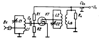
Encyclopedia of radio electronics and electrical engineering / RF power amplifiers Class A power amplifiers are rarely used. Basically, these are amplifiers of HF radio receivers with a large overload capacity. A practical diagram of such an amplifier is shown in Fig. 1. The input L1C1 circuit and the output L2C2 circuit are usually synchronously tuned and tuned to the frequency of the input signal.
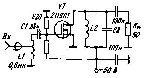
Equivalent resistance Re of the output circuit Re=P2p2/(RL+Rн'), where р=Sqr(L2/C2), Rн' - load resistance introduced into the oscillatory circuit; RL - active loss resistance; P2 - circuit inclusion coefficient. The value of Rn'=Rn/n22, where n2 is the transformation ratio. The quality factor of the output circuit when it is fully turned on Q=ReRi/(Re+Ri)2pfoL2 decreases due to the shunting effect of the output resistance of the transistor Ri. For powerful MIS transistors, Ri is small and usually does not exceed tens of kilo-ohms. Therefore, to increase Q2, an incomplete inclusion of the circuit is used. The bandwidth of the output circuit is 2Df2=fo2/Q2, and the resonance frequency is fo2=l/2pSqr(L2C2). In the HF band, such an amplifier can provide up to several tens of Ki. An important indicator of the amplifier is the noise level. The noise properties of high-power MIS transistors are considered in [1]. Figure 2 shows a practical circuit of the PA on a powerful MIS transistor KP901A. Since the task of obtaining a small L2C2 frequency band was not set, the circuit is connected directly to the drain circuit and is shunted by the load Rн=50 Ohm. In class A, the amplifier had Ku=5(Ku=SRn) and Kp>20 at f=30 MHz. When switching to the nonlinear mode, the output power reached 10 W.
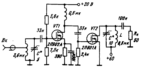
A two-stage PA (Fig. 3) is made on transistors KP902A and KP901A. The first stage operates in class A, the second in class B. To ensure class B, it is enough to exclude the divider from the gate value of the second transistor. The amplifier uses a broadband communication circuit between stages. At a frequency of 30 MHz, the amplifier provided Pout = 10 W with Ki> 15 and Kp> 100.
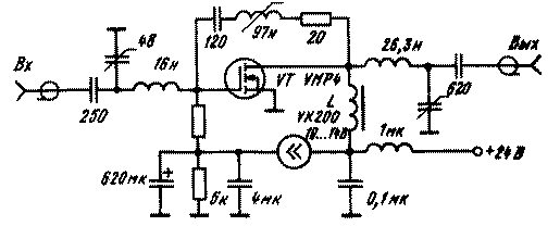
The narrow-band amplifier in Fig. 4 is designed to operate in the frequency range 144...146 MHz. It provides a power gain of 12 dB, a noise level of 2,4 dB and an intermodulation distortion level of no more than 30 dB.
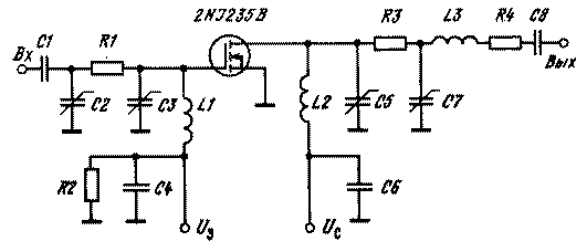
A resonant amplifier based on a powerful MIS transistor 2NS235B (Fig. 5) at a frequency of 700 MHz provides Pout = 17 W with an efficiency of 40 ... 45%.
The amplifier in Fig. 6 contains a neutralization circuit that reduces the level of backtalk to a level of -50 dB. At a frequency of 50 MHz, the amplifier has an increase in power of 18 dB, a noise level of 2,4 dB and an output power of up to 1 watt.
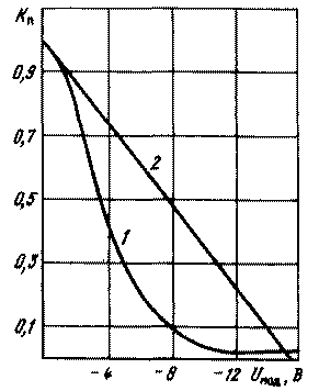
In the patented circuit in Fig. 7 (US Pat. No. 3.919563) at a frequency of 70 MHz, a real efficiency of 90% is achieved with an output power of 5 W at a frequency of 70 MHz. The quality factor of the output circuit is equal to 3.
Figure 8 shows a diagram of a three-stage PA based on domestic powerful MIS transistors KP905B, KP907B and KP909B.
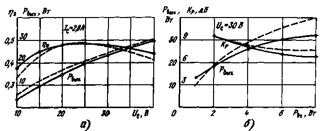
The amplifier delivers 30W of power at 300MHz. The first two stages use resonant U-shaped matching circuits, and the output stage uses an L-shaped circuit at the input and a U-shaped circuit at the output. The dependences of efficiency and Pout on Uc and Pout and Kp on Pin, obtained experimentally and by calculation, are shown in Fig. 9.
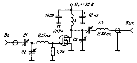
When using PA in AM radio transmitters (with amplitude modulation), there are difficulties associated with ensuring the linearity of the modulation characteristic, i.e., the dependence of Pout on the amplitude of the input signal. They are aggravated when using sharply non-linear modes of operation, such as class C. Figure 10 shows a diagram of a HF radio transmitter with amplitude modulation. Transmitter power 10,8 W when using a powerful UMOS transistor VMP4. Modulation is carried out by changing the bias voltage at the gate.
To reduce the non-linearity of the modulation characteristic (curve 1 in Fig. 11), the transmitter uses envelope feedback. To do this, the output AM voltage is rectified and the resulting low-frequency signal is used to create an OOS. Modulation response 2 in Fig. 10 illustrates a significant improvement in linearity.
Figure 12 shows a schematic diagram of a key PA with a rated output power of 10 W and an operating frequency of 2,7 MHz. The amplifier is made on transistors KP902, KP904. The efficiency of the amplifier at rated output power is 72%, the power gain is about 33 dB. The amplifier is excited from the K133LB logic element, the supply voltage is 27 V, the crest factor of the output stage drain voltage is 2,9. With a corresponding restructuring of the communication circuits, the amplifier with the given parameters operated in the range of 1,6 ... 8,1 MHz.
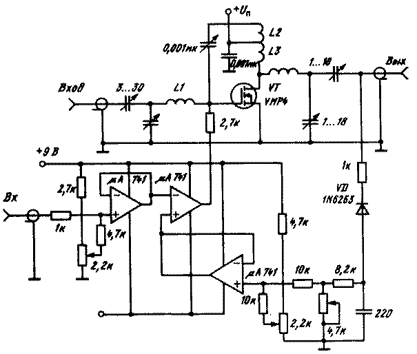
To provide a given power at higher frequencies, it is necessary to increase the exciter power. Structurally, both PAs were assembled on printed circuit boards using standard 100x150x20 mm radiators, which is explained by the standard dimensions of the PA unit in radio transmitters. Inductance coils in communication circuits are cylindrical on ferrite rods of the VCh-30 brand with a diameter of 16. The quality factor of the inductance coils is Q=150. Standard chokes with an inductance of 10 μH were used as blocking chokes in the power supply circuits of the drain of transistors of a one-watt amplifier and the preliminary stage of a 600-watt amplifier. The power inductor in the drain circuit of the KP904 transistor is on a ferrite ring, its inductance is 100 μH. Figure 13 shows a schematic diagram of a key PA with a rated output power Pout = 100 W, designed for use in unattended HF radio transmitters. The amplifier contains a pre-amplification stage, reverse on two KP907 transistors. At the input VT1, a matching U-shaped circuit C1L1C2C3 is included.
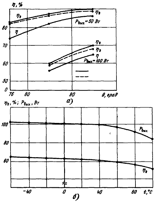
The final stage is assembled with six KP904A transistors. This number of transistors was chosen for reasons of increasing efficiency. Instead of KP904B transistors, you can also turn on six KP909 transistors or three more powerful KP913. The optimal key mode of the drain circuit is provided by a forming circuit containing elements C14, C15, C16, L7. The amplifier has a total efficiency = 62%. In this case, the electronic efficiency of the output stage is about 70%. The bridge circuit for switching on the transistors of the preliminary stage was used to maintain the efficiency of the amplifier (albeit with degraded parameters) in the event of an output transistor failure. For the same purpose, individual fuses are included in the sources of powerful transistors, the purpose of which is to turn off the faulty transistor. If, as a result of its breakdown, a mode close to the short circuit mode occurs in the transistor line, this makes the amplifier inoperable. Parallel connection of powerful MIS PT does not create additional difficulties in the calculation and tuning of the PA. The decrease in the efficiency of the amplifier compared to an amplifier of similar design (see Fig. 12) is mainly due to the use of power transistors in a 100-W amplifier. With a decrease in the output power level to 50 W, the efficiency of the amplifier increases to 85%, and the electronic efficiency to 90%. The values of the parameters of the elements shown in Fig. 13 correspond to a frequency of 2,9 MHz. The peak voltage factor at the drains of the KP904 transistors is 2,8, and the transistors themselves operate in a mode close to optimal. The crest factor of the drain voltage in the cascades on KP907 transistors is P = 2,1. The transistor operates in the key mode, however, the optimal mode is not ensured, since the optimal key mode for these transistors at Uc=27 V and cutoff angle φ=90° would be dangerous due to a significant crest factor at which the drain voltage could exceed the maximum allowable voltage equal to 60 V for the KP907 transistor. Figure 14, a shows the experimental and calculated curves illustrating the dependences of the efficiency, Pout and he on the drain current cutoff angle. The figure shows a good approximation of the calculated data to the experimental ones. It should be noted that the range of possible cutoff angles is quite narrow. An increase in the cutoff angles is prevented by a rapid increase in the crest factor of the drain voltage, and a decrease is prevented by an increase in the required excitation voltage, which quite soon begins to exceed Uad. together with the bias voltage Uz. Of course, with a decrease in the level of Pwt, the range of possible changes in the cutoff angles of the drain current expands.
The amplifier is made on a printed circuit board. As a heat sink, a radiator with dimensions of 130X130X50 mm is used. In the power supply circuits of KP907 transistors, standard DM-01 chokes with an inductance of 280 μH are used. Addition bridge chokes are wound on ferrite rings VK-30 dia.=26. The inductor in the power supply circuit of the output stage is wound on a ferrite ring VCh-30 dia. = 30. The inductor in the connection circuit of the output stage with the load is air, wound with silver-plated wire, diameter = 2,5, coil diameter 30 mm, L = 80 nH. The temperature dependences of the output power Pout and the efficiency of the key PA with an output power of 100 W are shown in Fig. 14b. It can be seen from the above dependences that in the range of -60...+60°C, the PA input power changes by no more than ±10%. The temperature also has a slight effect on the efficiency, which varies by ±5% in the indicated range. In this case, there is a drop in output power and efficiency with increasing temperature, associated with a decrease in slope 5 with increasing temperature. In the usual temperature range -60 ... +60 ° C, the change in he and Pout is insignificant, and this is achieved without any special measures for thermal stabilization of the CM. The latter is also an advantage of powerful MIS transistors. Literature:
Publication: N. Bolshakov, rf.atnn.ru
Artificial leather for touch emulation
15.04.2024 Petgugu Global cat litter
15.04.2024 The attractiveness of caring men
14.04.2024
▪ New series of tantalum capacitors ▪ African fish can't stand the heat ▪ Invulnerable displays from LG ▪ Smartphone Smartisan R1 with 1 TB of memory
▪ section of the site Microcontrollers. Article selection ▪ Soil article. consequences of soil pollution. Fundamentals of safe life ▪ article How are bricks made? Detailed answer ▪ article Wind in harness. Personal transport ▪ article Designs by S. Shipovsky. Encyclopedia of radio electronics and electrical engineering ▪ article Experiments with enzymes: oxidases and peroxidases. Chemical experience
Home page | Library | Articles | Website map | Site Reviews
www.diagram.com.ua |


 Leave your comment on this article: