|
|


 Arabic
 Bengali
 Chinese
 English
 French
 German
 Hebrew
 Hindi
Hindi Italian
 Japanese
 Korean
 Malay
Malay Polish
 Portuguese
 Spanish
 Turkish
 Ukrainian
 Vietnamese
|
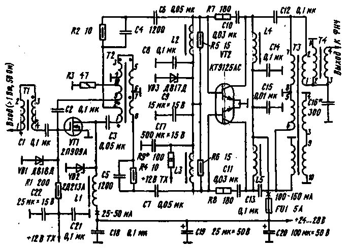
ENCYCLOPEDIA OF RADIO ELECTRONICS AND ELECTRICAL ENGINEERING Power amplifier for QRP transceiver. Encyclopedia of radio electronics and electrical engineering
Encyclopedia of radio electronics and electrical engineering / RF power amplifiers The amplifier is designed to work together with a low power transceiver (up to 1 W). Its schematic diagram is shown in fig. 1. It consists of two stages of amplification and provides output power up to 50 W in the frequency band from 3,5 to 30 MHz. The first stage is made on a field-effect transistor with an insulated gate 2P909A, operating in an undervoltage mode. The second stage is built on the KT9105AC transistor assembly, consisting of two silicon transistors, which have small dimensions, high reliability and low supply voltage. A feature of this amplifier is the simultaneous use of bipolar and field-effect transistors. This combination gives an improvement in noise characteristics and linearity in relation to the use of only bipolar transistors, and in comparison with the use of only field-effect transistors - an improvement in the energy characteristics of the amplifier.
The second stage is made according to the power addition scheme, which makes it possible to reduce unwanted fluctuations of the second and third order in the signal spectrum and is not particularly sensitive to load mismatch. In the amplifier, the cascades are well decoupled from mutual influence. In combination with the serial connection of transistors at the input and output in the second stage, at the same oscillatory power, the resulting input and load resistances increase four times. To increase the input and load resistance of the amplifier, transformers with a balanced input and output T2, T3 are included at its input and output. To switch to unbalanced external circuits, transformers T1, T4 with a turns ratio of 1:1 are used. The use of broadband transformers provides the necessary matching and allows you to work in the frequency band from 3,5 to 30 MHz without mechanical tuning. At the output of the amplifier, low-pass filter blocks are included. Transformer T1 is made on a ring (K10x5x3) magnetic core made of ferrite M400NN - M600NN. Its windings contain 12 turns. The winding is carried out with two bifilar twisted wires PEV-2 0,3, the T2 transformer is made on a ferrite (M600NN) ring of size K17x7x6. Winding 9-10, wound first, contains one turn of wire MGTF 12x0,075, the rest - 4 turns of bifilar twisted wires MGTF 12x0,075. Transformer ТЗ is made on the same magnetic circuit as Т2. Its windings contain 3 turns of bifilar twisted wires MGTF 19x0,12. Transformer T4 is made on two toroidal magnetic circuits 50VCh2, size K17x7x7. The winding is made with four wires MGTF 19x0,12 bifilar twisted (two per winding), the number of turns is 9. The pitch of the wires in all transformers is 5 mm. The inductor L1 - L5 is wound on a toroidal (K 10x6x3) magnetic core made of M1000NN ferrite. L1 contains 4 turns of wire PEV-2 0,3, L2, L3 (both on the same ring) - 3 turns each, - a L4, L5 (also on one ring) - 2 turns of wire PEV-2 0,49. Before winding, the rings of chokes and transformers are treated with a file and covered with nitro-lacquer or BF glue. You can also use ready-made chokes: L1 - inductance 15 ... 20 μH, L2, L3 - 10 μH, L4, L5 - 5 μH. The conductor connecting the gate of the transistor VT1 with other parts is passed through three ferrite (M1000NN) rings, the inner diameter of which is equal to the diameter of the wire. The same rings are installed at both ends of the conductor (three at each) going from terminal 9 of transformer T2 to capacitor C2. The magnetic cores are fixed with BF glue. The amplifier is mounted on a board with dimensions of 110x180 mm made of foil fiberglass with a thickness of 1,5 ... 2 mm. The dimensions of the board can be reduced if modern small-sized resistors and capacitors are used. First, transformers are installed on the board, the reliability of soldering and the absence of short circuits with a common wire on the board are checked. After that, the KT9125AC transistor is placed on the board, and then all the other details. During the final assembly, the reliability of fastening transistors, especially KT9125AC, to the heat sink is checked (it is installed on the side of the board free from parts, dimensions of at least 150x100 mm). Setting up the amplifier begins with checking the currents at the control points and selecting the appropriate resistors. The currents in each stage are set in the absence of an input signal. Capacitor C 16 is selected according to the maximum output power. When using the details indicated in the diagram, the frequency response of the amplifier turned out to be optimal for operation in the range of 3,5 ... 30 MHz. Author: Gennady Osipov (RV3AK), Moscow; Publication: N. Bolshakov, rf.atnn.ru
Artificial leather for touch emulation
15.04.2024 Petgugu Global cat litter
15.04.2024 The attractiveness of caring men
14.04.2024
▪ A battery the size of a grain of salt ▪ Electric liner for short flights ▪ The car will understand that the driver is talking on a mobile phone ▪ The air became heavier, the kilogram felt better ▪ Artificial intelligence has created a new material
▪ section of the site for the Musician. Selection of articles ▪ article What do digestives contribute to? Detailed answer ▪ article Water burner. home workshop ▪ article Generator ZCH. Encyclopedia of radio electronics and electrical engineering ▪ radio waves article. radio wave bands. Encyclopedia of radio electronics and electrical engineering
Home page | Library | Articles | Website map | Site Reviews
www.diagram.com.ua |

 Leave your comment on this article: