|
|


 Arabic
 Bengali
 Chinese
 English
 French
 German
 Hebrew
 Hindi
Hindi Italian
 Japanese
 Korean
 Malay
Malay Polish
 Portuguese
 Spanish
 Turkish
 Ukrainian
 Vietnamese
|
ENCYCLOPEDIA OF RADIO ELECTRONICS AND ELECTRICAL ENGINEERING Shortwave transceiver URAL-84. Encyclopedia of radio electronics and electrical engineering
Encyclopedia of radio electronics and electrical engineering / Civil radio communications The transceiver is designed for amateur radio communications in the short wave range of 1,8 ... 29 MHz. Type of work - telephone (SSB) and telegraph (CW). The transceiver is completely made on semiconductor devices and microcircuits, has a built-in digital scale (according to the scheme of a radio amateur V. Krinitsky (RA9CJL), published in this collection), a built-in power supply. The transceiver provides for the connection of an external GPA, which allows radio communications at separated frequencies. When developing the transceiver, the main attention was paid to obtaining high dynamic parameters of the receiving path and good ergonomic characteristics of the transceiver as a whole. The absence of an RF amplifier at the receiver input, the use of a high-level balanced mixer, a low-noise and linear IF path made it possible to accomplish the first task. The second problem was solved by using non-tunable band-pass filters at the receiver input, electronic range switching and the "transmit-receive" mode.
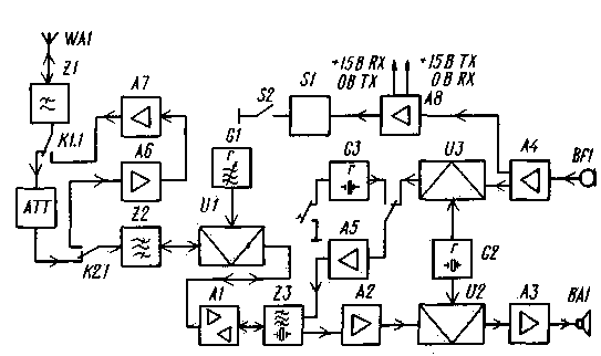
The transceiver (Fig. 1) is made according to the scheme with one frequency conversion. The choice of an intermediate frequency of 9100 kHz is determined by the presence of a home-made quartz filter made according to the method described in the Radio magazine No. 1, 2 for 1982 (it is possible to use an industrial quartz filter of the FP2P-410-8,815 type with minor changes in the circuit diagram). The common nodes of the transceiver in the receive-transmit mode are: low-pass filters Z1, band-pass filters Z2, mixer U1, reversible matching stage A1, smooth range generator G1, quartz filter Z3.
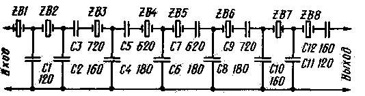
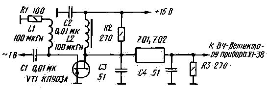
Connection of nodes for reception or transmission is made by relay contacts K1, K2, as well as by switch S1. The diagram shows nodes in receive mode. The signal from the antenna input through the low-pass filters Z1, the ATT step attenuator and the three-circuit band-pass filters Z2 is fed to the balanced mixer U1. Voltage is supplied to the same mixer from a smooth local oscillator G1. The converted signal passes through a reversible matching stage L / and then to a quartz filter Z3, is amplified by node A2 and enters the mixer U2, where it is mixed with the voltage from the reference crystal oscillator G2. The low-frequency signal from the mixer output goes to the low-frequency amplifier A3 and from it to the loudspeaker BA1. When switching from reception to transmission, the corresponding switching of functional units occurs. This is done either manually or by a voice control system. The signal from the BFJ microphone, amplified by node A4, goes to the voice control device A8, which in turn controls the switch S1, as well as to the mixer U3, which has voltage from the reference oscillator. The generated DSB signal is amplified by node A5, passes through a quartz filter Z3, where an intermediate frequency voltage of 9100 kHz with an upper sideband is selected, and enters through node A1 to mixer U1, the other input of which is supplied with a smooth local oscillator voltage. The signal of the operating frequency selected by band-pass filters Z2 from the output of the mixer U2 is fed to amplifier A6 and then, amplified in power at node A7, through the low-pass filter Z1 is fed to antenna WA1. The formation of a telegraph signal in the transceiver is performed using a manipulated generator G3, which is connected to node A5, instead of a single-sideband signal shaping device. The transceiver is made according to the block principle. In the diagram, the numbering of elements in each block is different. The main board (node A6, Fig. 2) contains a reversible mixer, a matching stage, a receiver IF path, quartz filters, a mixing detector, a receiver low-frequency amplifier, an AGC circuit, and a broadband smooth local oscillator voltage amplifier. Fig. 2a. Schematic diagram of the main board of the transceiver (node A6) Fig. 2b. Schematic diagram of the main board of the transceiver (node A6) The high-level passive mixer VD1 - VD8, T2, T3 is assembled according to a double balanced scheme. Its feature is the use of broadband transformers with a volume short-circuited turn (the design is described in the Radio magazine No. 1, 1983). In the case of using modern high-frequency diodes of the KD514A type in the mixer (and even better diodes with a Schottky barrier of the AA112 type), the signal loss in it will be about 4 ... 5 dB. The received signal is fed to the primary winding L3 of the transformer T2. The converted signal is taken from the midpoint of the winding L4. The voltage of the smooth local oscillator is amplified by a broadband amplifier based on the transistor VT1 and is fed to the input winding L7 of the transformer T3. On a powerful field-effect transistor VT2, a mixer matching cascade with a quartz filter is assembled. The KP905 type transistor was chosen due to its good noise parameters and linearity. When receiving, the cascade operates as an amplifier with a common gate and a gain of about 12 dB, its input impedance has an active character and is constant over a wide frequency range. Coordination with an eight-crystal SSB quartz filter at a frequency of 9100 kHz is provided using an L12 autotransformer. Schemes of quartz filters ZQ1 and ZQ2 are shown in fig. 3 and 4.
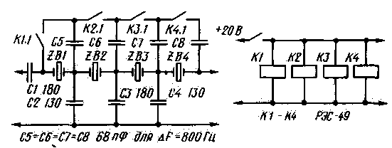
The ZQ1 filter has the following parameters:
If quartz resonators from the Granit radio station with frequencies of 1 ... 9000 kHz are used in the ZQ9150 filter, then the capacitance values in the filter circuit may remain unchanged. In the ZQ2 filter, the bandwidth can be changed. In SSB mode, it is 2,3 kHz, and in CW mode, when 68 pF capacitors are connected in parallel with the quartz resonators, the bandwidth narrows to 800 Hz. When transmitting, the cascade on the transistor VT2 is a source follower. The operation mode of this cascade is reversed by switching voltages from the control buses. When receiving +15 V in the Rx bus, 0 V in the Tx bus. When transmitting 0 V in the Rx bus, +15 V in the Tx bus. Diode keys VD9 and VD10 connect the "hot" end of the autotransformer L12 to the drain of the transistor when receiving or to its gate when switching to transmission. The grounding of the "cold" end of the autotransformer L12 at high frequency during reception occurs through the diode switch VD10 and capacitor C5, during transmission - through the diode switch VD9 and capacitor C4. On transistors VT5, VT6, the first cascade of the IF is assembled, which has a gain of about 20 dB. P-circuit L17C29C30 allows you to match the transistors of the cascode circuit and carry out additional filtering of the useful signal. The cascade load is the L16C26 circuit. Coordination with the second quartz filter ZQ2 is carried out using the coupling coil Lsv. This filter is a 4-crystal ladder filter with a 3dB bandwidth of 2,6kHz. In the mode of receiving telegraph signals, it is switched using a relay of the RES-49 type to a narrow band of about 0,7 kHz by connecting capacitors equal to about 68 pF in parallel with the quartz filters. The use of two quartz filters ZQ1 with a bandwidth of 2,4 kHz and ZQ2 significantly improved the suppression of signals outside the "transparency" of the filters, which reached 100 dB. The main signal amplification is performed in a cascade on the DA1 K224UR4 chip (K2US248 is the old designation). The mixing detector on transistors VT8, VT9 has no special features. Between the detector and the input of the low-frequency pre-amplifier on the DA2 chip, a ZQ3 type D3,4 low-pass filter (from Granit radio stations) is connected, which improves the noise and selective parameters of the receiving path. The ULF output stage is assembled according to the usual scheme on transistors VT15, VT16, VT17. An electronic key is assembled on the VT14 transistor, with the help of which the ULF input is shunted in the transmission mode. In telegraph mode, this key is closed, which allows you to listen to the self-control signal during transmission. The AGC circuit consists of a pre-amplifier AGC DA3, VT13, an emitter follower VT12, AGC detectors VD18, VD19 and VD24. An auxiliary "quick discharge" circuit with a discharge time of about 11 s is assembled on the VT17 transistor and the VD0,2 diode. When a useful signal is received, the AGC discharge time is determined by the main R36C53 chain. When the signal disappears, C53 is quickly discharged through the VD17 diode and the VT11 transistor. From the source follower VT10, the positive AGC voltage, which increases with increasing signal strength, is applied to the control transistors VT4 and VT7, which control the gain of the IF stages. To implement the AGC delay, the source of the transistor VT6 is connected to a reference voltage source collected on the zener diode VD11 and resistor R25. In the transmission mode, the switching voltage +4 VTX-O BRX is applied to transistors VT7, VT15, which practically closes the receiver's IF path. An adjustable amplifier is assembled on the VT3 transistor, operating in the SSB or CW signal transmission mode. The cascade gain is adjusted by changing the voltage at the second gate VT3 and reaches a depth of more than -40 dB. If desired, the ALC voltage can be applied to the second gate of this transistor. During transmission, the manipulated telegraph signal is amplified by the VT3 transistor, passes through the L15C22 circuits and parasitic capacitances of the receiver's closed IF path, is mixed in the detector with the reference local oscillator signal and enters the ULF for self-control. From the same circuit, the SSB or CW signal passes through the ZQ1 quartz filter, enters the VT2 matching stage, which in this case works as a source follower, and then to the VD1 - VD8 mixer, which transfers the signal to the operating frequency. The converted signal is taken from the winding L3 to the bandpass filter of node A2. Node A2 (Fig. 5) contains: a step attenuator of the receiver, a switching relay K17, band-pass filters, and preliminary stages of the transmitter. In the receive mode, the signal from node A1 is fed to an attenuator made on two resistor, P-links: R1R2R3, providing attenuation of 10 dB and R4R5R6 - 20 dB. The attenuator is controlled by a switch on the front panel of the S7 "ATT" receiver, which has the positions "0", "10 dB", "20 dB", "30 dB". P-links are switched by relay contacts K13 - K.16 type RES-49 (RES-79). After the attenuator, the signal passes through the normally closed contacts of the relay K17 (RES-55A) and enters the three-circuit band-pass filters, the selection of which is made by six push-button switches "Range" (SI - S6) with dependent fixation. Switching of range filters is carried out using relay K1 - K12 type RES-49 (RES-79). Band-pass filters suppress the image channel by more than 80 dB. Fig. 5. Schematic diagram of the pre-amplifier power and bandpass filters (node A2) The use of a relay for switching bandpass filters and an attenuator is due to the desire to achieve the highest possible dynamic range, while switching using diode switches (pin diodes, etc.) is not justified due to a significant decrease in the dynamic range and an increase in the noise of the receiving path. After the bandpass filters, the signal enters node A6, discussed earlier. In the transmission mode, the SSB or CW signal voltage coming from node A6 passes through band-pass filters in the opposite direction and through the contacts of relay K17 enters a broadband amplifier made on microwave transistors VT2, VT3, VT4, where it is amplified to a level of 5 ... 7 In eff. with unevenness in the range from 1,8...35 MHz no more than 2 dB. The load of the preamplifier is a broadband transformer 77 with a volume short-circuited turn, similar to the mixer transformers in node A6. Broadband transformer T2 is made of 16 ferrite rings, put on a copper tube (the design is described in the magazine "Radio" No. 12 for 1984). The R10R11C6 and R23C14 chains carry out the frequency response of the preamplifier. Resistors R13, R24 are selected according to the minimum output voltage unevenness over the entire range of amplified frequencies. The cascade on the transistor VT1 is an electronic key with a delay necessary for switching the antenna circuit at node A1. Node A1 - transmitter power amplifier (Fig. 6) made on a powerful field-effect transistor VTI type KP904A. There are also low-pass band filters (P-circuit), switched relays of the RES-10 type. The signal voltage at the operating frequency from the preamplifier is applied to the gate of the VTI transistor and amplified to an output power of about 30 watts. The load of the cascade is a broadband transformer made on a ferrite ring with a permeability of 300 NN and a diameter of 32 mm according to a well-known technique. The maximum drain current of the transistor reaches 2 A. Through the contacts of relay K13, closed during transmission, the amplified signal passes through a low-pass filter and enters the antenna (connector XI). Resistor R5 is used to set the initial current of the transistor. Through the R7C31 chain, a frequency-dependent OOS is carried out. The power amplifier has a fairly good linearity. With the correct selection of the quiescent current, out-of-band emissions are suppressed to -50 dB. In the reception mode from socket XI, the signal passes through the range low-pass filter and through the normally closed contacts of the relay K13 (type RES-55A) enters the range bandpass filters (node A2). As practice has shown (more than 6000 connections have been made on the transceiver), fears that relatively low-power relays in the power amplifier will often fail are unfounded, since all their contacts switch in the absence of a signal. Smooth range generator - node A3 (Fig. 7) consists of six separate range generators, switched by power supply in the second direction (the first is for switching band-pass filters) of pushbutton switches S1 -S6. On the field-effect transistor VTI, the generator is assembled directly according to the inductive three-point circuit. Transistor VT2 - emitter follower. The load of all six emitter followers is resistor R6. The voltage drop across it, equal to about +5 V, closes the emitter junctions of non-working repeaters, thereby excluding the influence of other range generators on the frequency of the running generator. ..Distribution of GPA frequencies by ranges and circuit data are given in Table. 1. GPA frequencies are selected in such a way that when changing the band, the desired sideband is automatically selected. Using the relay K1, K2 (RES-55A), an external GPA can be connected to the transceiver. The absence of mechanical switching, as well as the presence of separate circuits for each range, with their careful thermal compensation, made it possible to achieve good stability without resorting to frequency multiplication. This construction of the local oscillator allows you to optimize the levels of output voltages, create frequency overlap, and make the detuning value independent for each range. Table 1
The SSB and CW signal voltage conditioner - node A4 is shown in fig. eight. A reference crystal oscillator with a frequency of 9100 kHz is assembled on the VTI transistor. Transistor VT2 is a buffer stage, from which the reference oscillator signal is fed to a balanced modulator on varicaps VD1, VD2 and transformer T1. The modulator has a high linearity and allows you to suppress the carrier frequency by at least 50 dB. The cascade on the DA1 chip [is a microphone ULF, from the output of which the amplified low-frequency voltage is supplied to the midpoint of the L3 winding of the balanced modulator and through the VT6 emitter follower to the voice control system (VOX). The cascade on the transistor VT5 is a manipulated telegraph local oscillator stabilized by ZQ2 quartz. Its frequency is 800 ... 900 Hz higher than the frequency of the reference local oscillator, i.e., it coincides with the "transparency" band of the ZQ1 quartz filter. Depending on the type of work, telephone or telegraph, the emitter follower VT4 is supplied through the contacts of relay K1 with voltage either from a balanced modulator (SSB) or from a telegraph local oscillator (CW). From the output of transistor VT4, the signal is supplied for further conversion to node A6 (main board). Using the tuning resistor R21, the necessary gain of the ULF microphone is set, using the resistors RI8, R15, the carrier frequency of the reference local oscillator is balanced. Inductance L1 serves to fine-tune the frequency of the reference local oscillator on the lower slope of the ZQI crystal filter. The operation of the transceiver in the "reception" or <transmission" mode is controlled by the switch - node A7 (Fig. 9). The switch itself is made on powerful transistors VT5 - VT9. Transistors VT1. VT3, VT4 are included in the VOX system. VT7 - Anti-VOX. C using the trimmer resistor R1, the response delay of the voice control system is set, and RIO is the threshold for the response of the VOX system. Resistors R14 sets the threshold for the Anti-VOX system. The transistors VT10 - VT12 are equipped with a +9 V smooth local oscillator voltage regulator. An amplifier S- is assembled on the transistor VT13 meter In reception mode, the AGC voltage from the main board is supplied to its input through the diode VD7, and through the diode VD8 the voltage from node A1, proportional to the drain current of the powerful transistor VT1. . The commutator can be controlled from a pedal that is connected to pin 9 of the XI connector in both SSB and CW mode. In CW mode, positive pulses, which are applied to pin 7 of connector XI from an electronic automatic telegraph key, affect the voice control system, i.e., half-duplex operation of the transceiver can be performed. Voltages +15 V TX - O V RX are taken from pins 1,3 of connector X1 and fed to the transceiver nodes. Stabilizers +40 V and +15 V in the power supply (Fig. 10) made according to known schemes and protected by current. The connection diagram of the transceiver nodes is shown in fig. eleven. The frame is made of duralumin sheets 5 mm thick, connected with M2,5 screws at the end. The front and rear panels have dimensions of 315X130 mm and are fastened together by two sidewalls of 270X130 mm. The sidewalls are installed at a distance of 40 mm from the edges of the front and rear panels, forming cellars in which printed circuit boards are placed: on the left - the A2 node board, on the right - A7, A5 nodes (electronic telegraph key). Between the sidewalls at a height of 40 mm from the lower edge of the front and rear panels, a sub-chassis measuring 225X150 mm is fixed. Boards of local oscillator A2 and shaper A4 are installed on top of it. Below in the basement there is the main board A6, and between the sidewalls at a height of 25 mm from the lower edges of the front and rear panels there is a second subchassis 225X80 mm in size. It has a power supply transformer on the top right, and a +40 V and +15 V stabilizer board on the bottom, in the basement. Figures 12, 13 and 14 show the dimensions of the front, front and rear panels of the transceiver. The power amplifier assembly is located in a 115x90x50 mm shielded box, which is attached, along with the power transistor of the output stage, to the left above the second subchassis to the rear panel of the transceiver. On the rear panel, there is a radiator with 29 ribs 15 mm high for powerful output stage transistors and voltage stabilizers. The dimensions of the radiator are 315x90 mm. Fig.12. Transceiver front panel Fig.13. Front panel of the transceiver Fig.14. Rear panel of the transceiver Boards of nodes A2, A4, A5, A6, A7 are removable. They are connected to the wiring harness using connectors of the GRPPZ-(46)24SHP-V type. The smooth local oscillator board is housed in a shielded box. The main board A6 is made of double-sided fiberglass with a thickness of 1,5 ... 2 mm and dimensions of 210X 137,5 mm. The foil layer on the side of the parts is not removed. The conclusions of the parts connected to the case are soldered to the foil on both sides of the board, forming a common "ground". The remaining holes on the side of the parts are countersunk to prevent a short circuit to a common wire. The printed circuit board of node A6 is shown in fig. fifteen Quartz filters are made in. separate shielded and well-soldered brass boxes on B1 resonators from Granit radio stations. On fig. 16, 17 shows the printed circuit boards of the A4 and A7 nodes and the placement of elements on them. Variable capacitor - six-section from the R-123 radio station. The local oscillator circuits are located directly in the capacitor sections separated by partitions. It is possible to use variable capacitors from R-108 radio stations. In this case, two capacitors are taken, and using the existing gear, they are synchronously connected to each other, allowing you to create an eight-band GPA. The transceiver uses fixed resistors of the MLT-0,125 (MLT-0,25) type, tuning resistors of the SP4-1 type. Relay - RES-55A (RS4.569.601), RES-10 (RS4.524.302), RES-49 (RS4.569.421-07). Variable resistors type SPZ-12a. Capacitors type KM, KLS, K50-6. 50 μH high-frequency chokes are wound on F-1000NN K7X4X2 ferrite rings and have 30 turns of PELSHO 0,16, and 100 μH chokes have about 50 turns. Bandpass filter circuit data is given in table 2. The diameter of all coils here is 5 mm, the core is SCR type SB12A. Table 2
В table 3 winding data of other elements are given. Table 3
The contours of the band-pass filters are placed in aluminum screens with dimensions of 20x20 mm and a height of 25 mm. The power supply transformer with an overall power of about 70 W is wound on a tape ring magnetic circuit OL50 / 80-40. The primary winding is wound with PEV-2 0,41 wire and contains 1600 turns. The secondary winding is wound with PEV-2 1,5 wire and contains 260 turns. Transistor KP905 in node A6 can be replaced by KP903A. Transceiver setup. Before installing the elements on the boards, it is necessary to check their serviceability. First, each board is configured separately. For this, a separate power source and the necessary devices are used. It is advisable to carry out the setting in the following sequence : Node A7. The collector of the transistor VT1 is connected to a common wire and the resistor R7 is selected so that the residual voltage on the collector of the transistor VT6 is no more than +0,3 V. The connections are restored. The selection of resistors R8. R9 set on the VT9 collector a voltage close to zero, but not more than +0,3 V. Pins 1, 3 on connector XI must be loaded when tuned to resistors with a resistance of about 30 ohms and a dissipation power of at least 5 watts. Node A3. The establishment of range generators consists in setting the generating frequency indicated in Table. 2, using capacitors C2, C3 and the number of turns of inductance L1 (the tap from the coil is taken from 1/4-1/5 of the turns). Capacitor C4 is selected to be minimal, controlling the generation stability. The selection of C5 sets the required frequency detuning. In conclusion, a thorough thermal compensation of the circuit is carried out using a capacitor C3, made up of groups with different TKE. The GPA box during thermal compensation heats up to 35...40 °C. The output voltage across the resistor R6 should be 0,15 ... 0,2 Veff. Node A4. The RF voltage at the drain of the transistor VT3, supplied to the modulator, should be about 2 Veff. The LF voltage at the output of the DA1 microcircuit should be 1 ... 1,5 A, when voltage is applied to the microphone input from a sound generator with a frequency of 1000 Hz and an amplitude of 3 ... 5 mV. The modulator is configured as follows: first, by connecting an RF millivoltmeter to the VT4 emitter, using C26, the L3C26VD1VD2 circuit is tuned to resonance to the maximum signal. Then, the input of the microphone amplifier is short-circuited and, by sequential adjustment of resistors R18, R15, the modulator is balanced for maximum suppression of the carrier frequency at the minimum RF voltage at the VT4 emitter. Setting the manipulated oscillator is to set the frequency of the ZQ2 crystal oscillator. It must be higher than the reference oscillator frequency by 800...900 Hz (controlled by a frequency meter on pins 5, 28 of connector XI). The value of the output voltage at this point should be about 0,3 V, .. both in telegraph and telephone mode (when pronouncing a loud "a ... a"). At the output of the emitter follower VT2, the reference oscillator voltage should be 1,5 ... 1,8 Veff. Node A6. The board setup starts with the ULF receiver. Its sensitivity should be 5...10 mV at normal output volume. The detector VT8, VT9 is balanced when the reference local oscillator voltage is applied and the input is shorted by adjusting the resistor R31 to minimize noise at the IF output. The setting of the IF has no special features and consists in setting the circuits to the average frequency of the quartz filter (with the AGC system disabled, pin 11 of connector X1 is shorted to ground). At the output of the AGC system (pin 13 of connector XI), the constant voltage should reach a positive value of about +5 V when a voltage of about 75 ... 30 mV is applied to its input (capacitor C40) from the sound generator. The GPA voltage supplied to the balanced modulator (on the L7 winding) should be 1,3 ... 1,5 Veff. When transmitting, the voltage of the SSB or CW signal at the source of the transistor VT2 should not exceed 0,3 Veff. Constant voltages on the collectors of transistors VT4 and VT7 have a value of +9 V and +2,6 V, respectively. In this case, the GPA voltage must be applied to the mixer. When an input signal is applied to the L3 winding from an RF generator with a value of about 1 mV, the voltages on the collectors of these transistors decrease to +0,4 V and +0,3 V, respectively. The AGC system is turned on. After setting up the main board, its sensitivity from the input should be 0,2 ... 0,3 μV. Particular attention should be paid to the alignment quartz filters with IF stages. When setting up quartz filters, it should be taken into account that their parameters are highly dependent on the capacitances of the measuring circuit connected in parallel with the inputs and outputs of the filters. For this reason, it is recommended to adjust the filters using the measuring circuit shown in fig. 18. In this case, the capacities C12 in the eight-crystal and C4 in the four-crystal filters must be temporarily unsoldered.
Node A2. Band-pass filters are tuned according to a well-known technique, but in this case it is necessary to load their inputs and outputs with 75 ohm resistors. A broadband amplifier based on transistors VT2, VT3, VT4 is first tuned for direct current. The constant voltage on the VT3 collector is +15 ... 20 V, the quiescent current of the transistor should be about 70 ... 80 mA. Then, using resistors R13, R24, the unevenness of the output voltage is checked and selected when a band-pass filter from the GSS is supplied with a signal of 100 ... 150 mV in the range of 1,8 ... 30 MHz. At the same time, a capacitance of about 24 pF is connected in parallel to the resistor R270 (the input capacitance of KP904A is simulated). The RF output voltage should be 5-7 Veff. Node A1. The equivalent of a 75 Ohm antenna with a power of at least 30 W is connected to the output of the cascade and the value of the output power is checked. Bandpass filters must be pre-tuned using the "cold" tuning method. The "rest" current of the KP904A transistor should be about 200 mA. Its setting is made by potentiometer R5. After careful adjustment of individual nodes, a comprehensive tuning of the transceiver is carried out in all operating modes - "reception", "transmission", "tone". Literature:
Author: A. Pershin UA9CKV; Publication: N. Bolshakov, rf.atnn.ru
The world's tallest astronomical observatory opened
04.05.2024 Controlling objects using air currents
04.05.2024 Purebred dogs get sick no more often than purebred dogs
03.05.2024
▪ The magnet turns the material from soft to hard ▪ Spent spacecraft stages are returning ▪ ASUS VX279H-J and VX239H-J monitors
▪ site section Lighting. Article selection ▪ article They will argue, make some noise and disperse. Popular expression ▪ article by Badkhyz. Nature miracle ▪ article Power regulator for heaters. Encyclopedia of radio electronics and electrical engineering
Comments on the article: Leonid Great article! Thank you!
Home page | Library | Articles | Website map | Site Reviews
www.diagram.com.ua | |||||||||||||||||||||||||||||||||||||||||||||||||||||||||||||||||||||||||||||||||||||||||||||||||||||||||||||||||||||||||||||||||||||||||||||||||||||||||||||||||||||||||||||||||||||||||||||||||||||||||||||||||||||||||||||||||||||||||||||||||||||||||||||||||||||||||||||||||||||||||||||||||||||||||||||||||||||||||||||||||||||||||||||||||||||||||||||||||||||||||||||||||||||||||||||||||||

 Leave your comment on this article: