|
|


 Arabic
 Bengali
 Chinese
 English
 French
 German
 Hebrew
 Hindi
Hindi Italian
 Japanese
 Korean
 Malay
Malay Polish
 Portuguese
 Spanish
 Turkish
 Ukrainian
 Vietnamese
|
ENCYCLOPEDIA OF RADIO ELECTRONICS AND ELECTRICAL ENGINEERING Power amplifier KB transceiver. Encyclopedia of radio electronics and electrical engineering
Encyclopedia of radio electronics and electrical engineering / RF power amplifiers The described device allows linear amplification of power in the frequency range from 1,83 to 29,7 MHz. Its input and output impedance is about 50 ohms. The maximum input signal level is 150 mV (effective value). When it was tested by the two-frequency method, the power at a frequency of 14,1 MHz in the peak of the envelope at a load with a resistance of 50 Ohms reached 75 W, and the level of mutual modulation did not exceed 30 dB. In this case, the terminal stage consumed a current of 27 A from a voltage source of 5 V. The efficiency of the terminal stage when operating with a telegraph and power in a load of 40 W is 40%. The circuit diagram of the amplifier is shown in fig. one. The radio frequency signal from the transceiver or transmitter through the capacitor C1 and the open diode VD2 enters the base of the transistor VT2, on which the input amplifier stage is made. Negative frequency-dependent feedback in the emitter circuit affects the gain at a frequency of 22...24 MHz. A broadband transformer T1 is included in the collector circuit of the transistor. An input attenuator is assembled on resistors R7-R9. On the transistor VT3, a pre-terminal cascade is made, operating in class AB mode. The bias voltage is set by the VD3 diode. The quiescent current is set with a trimming resistor R16. To thermally stabilize the operation mode of the cascade, the VD3 diode has a thermal contact with the VT3 transistor. As the temperature rises, the direct resistance of the diode and the voltage across it decrease. This reduces the quiescent current of the transistor VT3. Resistors R19, R20 form a negative feedback circuit that increases the linearity of the frequency response and the stability of the cascade. If necessary, the frequency response can be adjusted by the elements C9, R18. The final stage is assembled according to a push-pull circuit on transistors VT4, VT5. Transformers T2 and T4 match the resistances of the input and output of the amplifier, respectively. Power is supplied to the collectors of both transistors through the windings II, III of the T3 transformer. Correction circuits C14C15R24R25R26 and C16C17R27R28R29 reduce the gain in the low-frequency region, and C12R23 and C20, together with winding 1 of the T3 transformer, raise the frequency response near the upper limit of the operating frequency range.
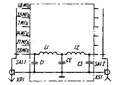
To stabilize the quiescent current of the transistors of the final stage, a parametric stabilizer is used on the VD4 diode and the collector junction of the VT7 transistor, which operates on the direct branch of the current-voltage characteristic. The emitter follower on the transistor VT6 amplifies the output current of the stabilizer. Transistor VT7, mounted on a heat sink between transistors VT4, VT5, performs the functions of a temperature sensor. Under normal conditions, the voltage drops to approximately 4 V on the VD7 and VT1,3 elements. As the heat sink heats up, the bias voltage of the terminal transistors decreases, which prevents the quiescent current of the VT4 and VT5 transistors from increasing. The collector current of the terminal transistors can be controlled by the voltage drop across the resistor R33. To do this, between points 6 and 7, it is necessary to turn on a microammeter (it can also be a device used in the S-meter of the transceiver) with a full deflection current of the needle of 100 μA. The cascade on the transistor VT1 performs the functions of an electronic switch that controls the input attenuator. If point 3 is not connected to a common wire, then the diode VD2 is open and current flows through it and resistors R1, R4, R8, R9. In this case, the transistor VT1 is in saturation mode. Diode VD1 is closed, and the attenuator is turned off. If point 3 is connected to a common wire, then the transistor will close. The voltage on its collector will increase to 6 V. At the same time, the VD1 diode will open and connect the input attenuator, and VD2 will close. In this mode, the output power of the amplifier is about 5 watts. The described method of power reduction does not affect the cascade mode and guarantees high frequency response linearity during QRP operation. By the way, it can also be used for emergency power reduction with increasing SWR in the antenna feeder. To do this, at the output of the transmitting path, it is necessary to install a reflected wave sensor with a threshold device, the output of which is connected to point 3. The final and final stages of the amplifier are powered from a source that provides a current of at least 5 A at a voltage of 27 V. To power the input amplifier and bias circuits, you need 12 V voltage source with an output current of at least 120 mA. To filter harmonics at the output of the amplifier, a low-pass filter is used (Fig. 2).
When switching from one range to another, it is possible to switch the filter links with both a jack switch and a relay (for example, RPA12, RPS2/7, RES47). The amplifier is built on printed circuit board made of double-sided foil fiberglass (Fig. 3). The location of parts is shown in Fig. 4. The device uses fixed resistors MLT-0,25, MLT-0,5 (R30, R31). Resistor R33 is made from a suitable piece of nichrome wire from a hotplate spiral. Trimmer resistors R16, R21, R34 - SPZ-19A. SPZ-27A, SPZ-38A are also suitable. Capacitors C13, C21, C24 - K50-6, K50-16, the rest - K10-7V or KM. Diodes KD409A are interchangeable with KD407A or, in extreme cases, with KD522B. Transistor VT1 - KT315 with any letter index, VT2 - KT610A or KT606A. In the pre-terminal cascade, you can use KT922B, in the terminal one - KT931A. KT956A and others with an output power of at least 70 watts. Transformer T1 is made on a ring (size K12X6X4,5) of ferrite 1000NN. The windings contain 10 turns each, they are wound simultaneously with two PEV-2 0,31 conductors twisted together. Twist pitch - 10 mm. The same rings are used in transformers T2 and T4 (Fig. 5).
In T4, five rings 3 are put on two brass tubes 2 27 mm long with an outer diameter of 6 and an inner diameter of 4 mm. Tubes with rings are inserted into the holes of the cheeks 1, 4 made of foil fiberglass with a thickness of 1,5 ... 2 mm. The ends of the tubes are flared and soldered. On one of the cheeks, the foil electrically connects the ends of the tubes, and on the other, it forms two platforms. Thus, the tubes, together with the conductive path on the cheek, form a volumetric coil, which is connected to the collectors of transistors VT4 and VT5. The output winding contains two turns. flexible insulated wire 5 with a cross section of 6,75 mm2, stretched inside the tubes. The T2 transformer is similarly arranged, only in it there are three rings on each tube (their length is 18 mm). The ends of the tubes are connected to the base circuits of the transistors VT4, VT5, and the ends of the winding containing two turns of an insulated wire with a cross section of 11 mm0,35 are connected to the capacitor C2 and a common wire. The T3 transformer is made on a ring (size K20X10X6) magnetic core made of 1000NN ferrite. 10 turns of two PEV-2 0,8 conductors twisted together (twisting pitch 10 mm) form windings II and III. Winding 1 is a coil of a mounting wire with a cross section of 0,12 mm, threaded through a hole in the magnetic circuit. Transistors VT3-VT5, VT7 are placed on heat sinks. The diode VD3, installed near the transistor VT3, is lubricated with a small amount of heat-conducting paste KPT-8 for better thermal contact.
The data of the LPF elements are given in the table. Its coils for the ranges of 14, 21 and 28 MHz are wound turn to turn with PEV-2 wire with a diameter of 1 mm, for the rest - 1,2 mm. Setting up the amplifier begins with checking the modes of transistors. Trimmer resistor R16 set the quiescent current of the transistor VT3 equal to 40 mA. Resistor R21 ensures that the quiescent current of the final amplifier is 100 mA. Then point 3 of the printed circuit board is connected to a common wire. A generator is connected to the input of the amplifier, and a low-pass filter with a load of 50 ohms is connected to the output. By applying a signal with a frequency of 29 MHz at a level of 50 mV, the voltage at the load is controlled. After that, the ends of the winding 1 of the transformer T3 are interchanged and the previous operation is repeated. In the future, the inclusion is used, in which the output signal level is greater. Next, the capacitor C20 is selected, achieving the maximum output voltage. Then you need to check the power in the remaining amateur bands. If the amplifier is not self-excited in any of them, remove the jumper between point 3 and the common wire and again control the power in each range. During the final check of the amplifier, an amplitude-modulated signal is fed to the input from the generator and the shape of the envelope is controlled on the load with an oscilloscope. It should not have visible distortion at all power levels. Using a two-frequency generator [1], step attenuator [2], spectrum analyzer [3, 4], it is possible to measure the level of intermodulation products and the relative value of out-of-band components. If we are talking about a power amplifier with excitation from a generator, then these will be only harmonics of the fundamental frequency. In the case of testing a finished transceiver in the spectrum, in addition to harmonics, there will be local oscillator signals and their harmonics, as well as many components that have arisen during signal conversion. In any case, they should not exceed -40 dB. Literature 1. Skrypnik V. Two-frequency generator. - Radio, 1985, No. 8, p. 22-23. Author: V. Skrypnik (UY5DJ), Kharkov; Publication: N. Bolshakov, rf.atnn.ru
Artificial leather for touch emulation
15.04.2024 Petgugu Global cat litter
15.04.2024 The attractiveness of caring men
14.04.2024
▪ AOC 24G15N 1080p Gaming Monitor ▪ The impact of hugs on stress levels ▪ Slim Full HD display from LG ▪ Improvement of iOLED technology
▪ site section Regulators of current, voltage, power. Article selection ▪ article Finance and credit. Crib ▪ article Who performed the first human heart transplant and when? Detailed answer ▪ article solar distiller. Travel Tips ▪ article Water in an upside down glass. physical experiment
Home page | Library | Articles | Website map | Site Reviews
www.diagram.com.ua | |||||||||||||||||||||||||||||||||||||||||||||||||||||||


 Leave your comment on this article: