|
|


 Arabic
 Bengali
 Chinese
 English
 French
 German
 Hebrew
 Hindi
Hindi Italian
 Japanese
 Korean
 Malay
Malay Polish
 Portuguese
 Spanish
 Turkish
 Ukrainian
 Vietnamese
|
ENCYCLOPEDIA OF RADIO ELECTRONICS AND ELECTRICAL ENGINEERING Production of printed circuit boards. Encyclopedia of radio electronics and electrical engineering
Encyclopedia of radio electronics and electrical engineering / Ham Radio Technologies Most of the designs for beginner radio amateurs remain in their dreams due to the fact that there are many problems with the manufacture of a printed circuit board, and many circuits cannot be implemented on the "weight". Recently, several methods for manufacturing printed circuit boards have become available to most radio amateurs. All methods differ from each other only in the way the pattern is applied to the board. Subsequent technological processes, such as etching the board, drilling holes, are no different. The simplest methods include the following: drawing a pattern by hand with varnish, paint, or sawing the tracks with a knife. Although these methods are simple, the manufacturing process is very slow and the quality of the resulting boards is often very low. To date, the following methods are the most optimal: laser-iron technology, photoresistive method (photolithography), marker method. These technologies will be discussed in more detail in this article. 1. Laser iron technology This technology is very simple at all stages and is as follows. In order to get conductors on a printed circuit board, you must first get a track pattern using some software product (Acel Eda, P-CAD, Sprint-Layout, etc.). Then you need to print the template on a laser printer and transfer it to foil fiberglass, attach it to the foil with a pattern and heat it with an iron. The toner from the template should stick to the board. After the template has stuck to the board, the paper on which it was made must be torn off. Where the toner film has turned out, there will be conductive paths, i.e. after etching, the copper under the toner will remain. I would like to note that it is best to use matte photo paper for inkjet printing to make a template, since it has a pressed finely dispersed absorbent layer that easily lags behind the base and, therefore, the quality of the image transferred to the board is quite high. The density of photo paper should be about 100-120 g/m3, photo paper with a lower density lags behind more easily, and the quality is excellent. The printer should have a resolution of 600 dpi, but it is better to use a printer with a resolution of 1200 dpi. After etching, the toner can be removed from the copper tracks with sandpaper (zeroing), but the easiest way to do this is with acetone or paint thinner. 2. Photoresistive method This method is based on photoresist, the use of which allows obtaining very high quality and stability in the manufacture of printed circuit boards. Today, the industry offers many different photoresist sprays. However, film photoresist is the cheapest and easiest to use. We will describe its application in more detail below. In practice, film photoresist of the LIUXI or PF-VShch type can be used. First you need to make a photomask, for this you need an inkjet or laser film (depending on the printer available), on which the printed circuit board pattern is printed. This photomask should be printed at maximum resolution and quality so that the ink layer is as thick as possible. The photomask is printed either positive or negative, depending on the photoresistive film used (negative photoresistive film is most often produced in the industry). Then, a photoresistive film is glued onto the prepared foil textolite (Fig. 1).
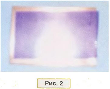
The photoresist film is covered with two protective films, one of which is matte (the photoresist has an adhesive base under it), and the other is glossy (protective). In order to glue the photoresistive film onto the textolite, it is necessary to carefully gradually peel off the matte film, gluing and smoothing the photoresist well so that there are no air bubbles under it (Fig. 2).
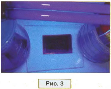
When the photoresistive film is glued onto the textolite, a photomask is superimposed on top of it, which is well pressed against the board with the help of ordinary window (transparent) glass. Next, it is necessary to expose the photomask (Fig. 3) to the photoresist, for which an ultraviolet lamp is usually used. The exposure time (determined experimentally) can vary from several tens of seconds to tens of minutes, depending on the emission spectrum of the lamp, the distance between the lamp and the board, and the type of photoresist.
After exposure, it is necessary to develop the photoresist in a 3-5% solution of soda ash. Before putting the board in a warm solution of soda ash, you must remove the protective film. During the development of the photoresist, it is necessary to constantly stir the soda ash solution. The development time is approximately 30-60 seconds, after which the unnecessary photoresist is washed off the board under a stream of warm water. In those areas where there should be conductive tracks, a photoresist film remains (Fig. 4).
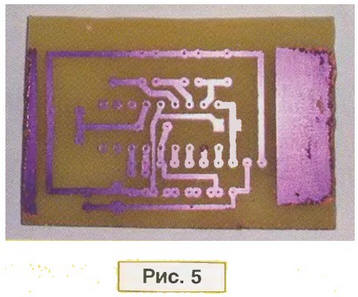
After etching the board (Fig. 5), the photoresist remaining on the tracks is removed with acetone or ammonia.
It should be noted that during all operations it is desirable that there is no access to sunlight, and lighting should be organized using fluorescent lamps, to which the photoresist practically does not react. Both in the first and in the second method, a solution of copper sulfate, ferric chloride, nitric acid, etc. can be used as an etchant. 3. Marker method Previously, the author, in the manufacture of printed circuit boards (PCB), fooled his head with varnishes, syringes, etc. Once it was necessary to put inscriptions on the glass. For this purpose, I purchased a marker made in Italy HI-TEXT 720P PERMANENT in a stationery store with a writing part diameter of 1 mm. While making the next power supply board, for the experiment I applied inscriptions to them on the workpiece. After etching the PCB, I was pleasantly surprised: the inscriptions did not wash off and were clearly printed on the board. Since then, I have been drawing any tracks with such markers, of any thickness and configuration (up to 0,1 mm). Errors are easy to correct with the 647th solvent. PP is made in the following way. I drill holes, I clean burrs. Then with a school rubber band, its hard part, I wipe the PP to a shine. I draw with a marker. Next, I carry out etching with a solution of the following composition: 4 tbsp. tablespoons of salt and 2 tbsp. spoons of copper sulfate, 0,5 liters of hot water 60 ... 80 ° C. I prepare the solution in a plastic container (plastic basin). PP persecution in a water bath for 10 ... 15 minutes (I lower a basin into a wide saucepan with water, the water in the saucepan should not boil, the basin sometimes needs to be rocked) - and the board is ready. This amount of solution is enough for a double-sided board with dimensions of 100x150 mm. Next, I rinse the PP with water and wash off Figure 647 with a solvent. Again I wipe the PP tracks with an eraser, cover them with liquid rosin and tin with a soldering iron. Then I wash off the rosin with a solvent (I check the quality of the tracks) and again cover it with liquid rosin - the board is ready for installation. During installation, I clean the conclusions of the parts with an elastic band. Literature, resources
Authors: E.Pereverzev Krasnodar Territory, Kropotkin; Yu.A. Kamyshansky, village Russkaya-Lozovaya, Kharkiv region
Artificial leather for touch emulation
15.04.2024 Petgugu Global cat litter
15.04.2024 The attractiveness of caring men
14.04.2024
▪ Dual Channel Isolated SiC MOSFET Drivers 2EDF0275F and 2EDS9265H ▪ GaAs-solar panels for roofs of electric vehicles ▪ A new method for fast optical distance measurement ▪ A new family of highly integrated real-time clocks
▪ section of the site For a beginner radio amateur. Article selection ▪ article Psychological help after situations with high danger to life. Fundamentals of safe life ▪ article Why did Theseus and Pirithous descend into the underworld? Detailed answer ▪ Article Leading Sales Manager. Job description
Home page | Library | Articles | Website map | Site Reviews
www.diagram.com.ua |


 Leave your comment on this article: