|
|


 Arabic
 Bengali
 Chinese
 English
 French
 German
 Hebrew
 Hindi
Hindi Italian
 Japanese
 Korean
 Malay
Malay Polish
 Portuguese
 Spanish
 Turkish
 Ukrainian
 Vietnamese
|
ENCYCLOPEDIA OF RADIO ELECTRONICS AND ELECTRICAL ENGINEERING Stroboscopic light-dynamic installation. Encyclopedia of radio electronics and electrical engineering
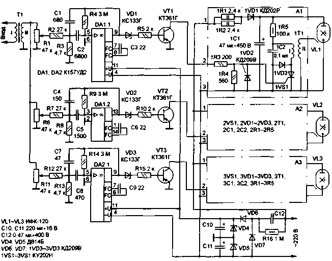
Encyclopedia of radio electronics and electrical engineering / Color and music settings A distinctive feature of the described light-dynamic installation is the use of special pulse lamps instead of conventional incandescent lamps. This eliminates the main disadvantage of such devices - high inertia. With its help, you can get excellent light accompaniment of musical works, as well as solve the problem with the design of discos, concert halls, living rooms. On the pages of "Radio" at different times, light-dynamic installations (SDUs) of varying degrees of complexity were described (for example, [1, 2]). All these devices use incandescent lamps switched by thyristors or powerful transistors. However, incandescent lamps have significant disadvantages: inertia and limited service life, which the proposed stroboscopic SDU is free from. It consists of a power supply unit and three active band-pass filters, three identical A1-AZ flash lamp control units are connected to their outputs (Fig. 1).
The power supply is a half-wave rectifier VD6, VD7 connected to the network through a ballast capacitor C12. The rectifier is loaded on the zener diodes VD4, VD5 and filter capacitors C10, SP, which form a bipolar voltage to power the operational amplifiers DA1, DA2. The use of a source with a ballast capacitor made it possible to significantly reduce the dimensions of the SDU. However, in this case, all structural elements have a galvanic connection with the network, which must be remembered during the establishment and operation. For the same reason, variable resistors must be provided with dielectric handles. The input signal from the line output of a tape recorder, radio or CD player is fed to the primary winding of the transformer T1, designed for galvanic isolation of the signal source from the SDU elements. If the input signal is small (less than 0,3 V), the transformer must be step-up and provide a voltage amplitude on the secondary winding of about 0,5 V. Then the signal is fed to the inputs of active band-pass filters through variable resistors, which set the optimum level. The filters are made on dual op amps DA1, DA2 and are borrowed from [1]. The method of their calculation has been repeatedly published on the pages of the journal, so it is not presented here. The SDU uses filters with the following parameters: gain at the resonant frequency - 40 dB; quality factor - 10; resonant frequencies - 680 Hz (upper in the circuit), 3000 Hz (middle) and 9800 Hz (lower). In general, the number of filters can be any and is limited only by the power of the power supply. For those wishing to rebuild the resonant frequencies, we give the following recommendations. By tuning the filter to a different resonant frequency, it is necessary to change the capacitance of the capacitors C1, C2 (C4, C5 or C7, C8). In order for the gain at the resonant frequency and the quality factor of the filter to remain the same, the ratio should be maintained: C2=10C1 (similar to C4=10C5, C7=10C8). Then, knowing the required resonant frequency fo, one can determine the capacitance value of one of the filter capacitors. So, for the top filter according to the scheme C1 =[( 1 /R2 + 1 /R3)/( 10R4)] ^/(6,28fo), where the capacitance of the capacitor C1 is in farads, the frequency fo is in hertz, the resistance of the resistors is in ohms. Similarly, the capacitance of the capacitors of other filters is calculated. Filter load - transistors VT1-VT3, connected with a common emitter. At a low level of the input signal or if its frequency does not fall within the passband of the filter, the amplitude of the filtered signal is insufficient to open the corresponding transistor. The voltage on its collector is about -8V. If, however, the signal at the filter input is of sufficient level and its frequency falls within the passband of the filter, the transistor opens with the amplitude of the negative half-wave of the filtered signal, and pulses of positive polarity are observed at its collector. In the circuits of the base of transistors VT1-VT3, subtractive zener diodes VD1-VD3 are connected in series, which increase the dead zone. The pulses from the transistors are fed to the blocks A1-AZ. Consider the operation of block A1. Blocks A2 and A3 work similarly. When there are no pulses, the storage capacitor 1C1 is charged to a voltage of about 300 V through resistors 1R1, 1R2 and a diode 1VD1. Since the 1VS1 trinistor is closed, the 1C2 capacitor is charged through the 1R5 resistor. A pulse of positive polarity coming from the collector of the transistor VT1 opens the trinistor, discharging the 1C2 capacitor to the primary winding of the 1T1 transformer. A high voltage pulse arises on its secondary winding, which "ignites" the flash lamp VL1. After the lamp flashes, the process of charging capacitors 1C1, 1C2 is repeated. Diodes 1VD2, 1VD3 protect the trinistor from reverse voltage. Note that both individual pulses and bursts of pulses can be formed on the collectors of transistors. In the latter case, the flash lamp will turn on only with the first pulse in the burst, which has an amplitude sufficient to open the trinistor. Since it takes a certain time to charge the storage capacitors 1C1, 1C2, subsequent pulses in the burst will not cause the flash lamp to flash. The SDU is mounted on four separate boards: blocks A1-AZ are assembled on three boards, and the rest of the elements are on the fourth board. This division into separate boards turned out to be quite convenient for the following reasons. To obtain the maximum effect from the light accompaniment, flash lamps must be spaced apart in space, for example, placed in the corners of the room. However, using long wires to connect flash lamps (one of which is high-voltage) is impractical and dangerous. It is much more convenient to spread the blocks A1 -A3 themselves. In addition, when they are located on separate boards, it is very easy to obtain both separate and interconnected stroboscopes. To do this, you need to connect the A1-AZ blocks to a simple digital device that generates a certain sequence of control pulses. A drawing of the main printed circuit board of the SDU is shown in fig. 2. In the holes circled by a semicircle, it is necessary to solder the jumpers connecting the upper and lower printed conductors. A drawing of the printed circuit board of A1-AZ blocks is shown in Fig. 3. Instead of the K157UD2 chip, you can use the op-amp of the K140, K153, K544, K553 series. Pay special attention to corrective circuits. Transistors - any of the KT361, KT3107, KT502 series; diodes VD6, VD7, 1VD2-3VD2, 1VD3-3VD3 - series KD209, KD105 with letter indices B-G; zener diodes VD4, VD5 - D814A-D814G, VD1-VD3 -KS133A-KS147A; trinistors - KU202M, KU202N. Resistors - MLT, variables - SDR, SPO or similar. Capacitors C12, 1C2-ZC2 - K73-17 for a voltage of at least 400 V; C10, C11 -K50-35, K50-16; 1S1-ZS1 - K50-27 or others for voltages over 350 V; the rest - any ceramic. Transformer T1 - TOT-64 or other small-sized one. Transformers 1T1-ZT1 are wound on wooden frames with a rod diameter of 10 mm, a cheek diameter of 20 mm and a distance between the cheeks of 10 mm. The magnetic circuit is not used. First, the secondary winding is wound with a PEV-2 0,1 wire. The fastest and easiest way to make a transformer is with an electric drill. There is no need to specifically count the number of turns of the secondary winding: it is wound almost until the frame is completely filled. The winding should be impregnated two or three times with molten paraffin to prevent high-voltage breakdowns between the turns. After the insulation layer, the primary winding is wound, containing 10 ... 20 turns of PEL or PEV-2 wire with a diameter of 0,3 ... 0,6 mm. It is necessary to pay attention to the type of wires for connecting flash lamps. The wires coming from the secondary winding of transformers 1T1-3T1 must have good insulation. You should also avoid twisting it with other wires. The total length of the wires must not exceed one meter. In conclusion, some recommendations for the establishment of CDS. First you need to set the sliders of variable resistors to the lower position according to the diagram. Then, after applying the input signal, slowly rotate the slider of the resistor R1. At the moment the VL1 lamp is turned on, the position of the variable resistor slider should be fixed. Set up other channels in the same way. One feature of the SDU should be noted. With a significant increase in the input signal level, as well as in the case of an overestimated signal level at the input of at least one filter, the flash lamps will be absent. To reduce the current surge when the device is connected to the network, it is advisable to include a resistor with a resistance of 12 ... 36 Ohm in series with the capacitor C47. The insulation of the windings of the transformer T1 must be designed for a voltage of at least 300 V. It is better to wind it yourself, and securely insulate the windings. The common wire of the device must not be connected to the housing. Literature
Author: A. Tarazov, St. Petersburg; Publication: N. Bolshakov, rf.atnn.ru
Machine for thinning flowers in gardens
02.05.2024 Advanced Infrared Microscope
02.05.2024 Air trap for insects
01.05.2024
▪ Antimatter falls down like normal matter
▪ section of the site The most important scientific discoveries. Article selection ▪ article Libation to Bacchus. Popular expression ▪ article What is osmosis? Detailed answer ▪ article Car Kozlik. Personal transport ▪ article Vertical top food. Encyclopedia of radio electronics and electrical engineering ▪ article Charger. Encyclopedia of radio electronics and electrical engineering
Home page | Library | Articles | Website map | Site Reviews
www.diagram.com.ua |

 Leave your comment on this article: