K1464CA1 - two voltage comparators with an open collector output. Reference data

Encyclopedia of radio electronics and electrical engineering / Reference materials
 Comments on the article
In the case of this microcircuit there are two independent (connected only by power circuits) comparators. Each of them is capable of operating in a wide range of input voltage values, is powered by both unipolar and bipolar sources, and has an open-collector output. Pn-p transistors work in the input stages of the comparators, so the input current is flowing. The input current is practically independent of the state of the output and the load resistance.
The advantages of comparators should also include a relatively low current consumption and the ability to compare input signals that are close to zero in voltage. The microcircuit can be used in pulse generators, analog-to-digital converters, high-voltage logic elements, pulse detectors, and other nodes. In terms of output voltage levels, comparators are compatible with TTL, DTL, ESL and CMOS elements.
The devices are packaged in a plastic eight-pin package of two types: 2101.8-1 (DIP-8) - K1464CA1R for traditional mounting and 430310.8-A (SO-8) - K1464CA1T, for surface mounting. The housing drawings are shown in fig. 1, a and b. In terms of electrical characteristics, both microcircuits are identical. The foreign analogue of the K1464CA1 chip is the LM393 (National Semiconductor Corporation).

The pinout of the microcircuit is shown in fig. 2

Basic electrical characteristics
Input bias voltage, mV, max, at 5 V supply voltage and temperature*
- +25 °С......7
- -40...+85°С......9
Input current, nA, no more, at a supply voltage of 5 V and temperature
- +25 °С......250
- -40...+85°С......400
Difference of input current values, nA, no more, at supply voltage 5 V and temperature
- +25 °С......50
- -40...+85°С......150
Input common-mode voltage limits, V, at 30 V supply voltage and temperature
- +25 °C......0...(Unt1T-1,5B)
- -40...+85°С......0...(supply-2V)
Current consumption, mA, no more, with an unconnected output, temperature +25 °C and supply voltage
- Output current (sinking), mA, not less, at a voltage at the inverting input of 1 V, zero voltage at the non-inverting input, an output voltage of not more than 1,5 V, a supply voltage of 5 V and a temperature of + 25 °C.... 6
- Saturation voltage, mV, not more than, at voltage at the inverting input 1 V, zero voltage at the non-inverting input, output current not more than 4 mA, supply voltage 5 V and temperature 25 °С......700
- Output leakage current, μA, no more, at a voltage at the non-inverting input of 1 V, zero voltage at the inverting input, an output voltage of 30 V and a temperature of 25 °C......1
- Supply voltage, V, unipolar......2...36
- bipolar......2x1...2x18
- Differential input voltage, V......0...36
* Everywhere ambient temperature.
Limit values
- The highest supply voltage, V ...... 40
- Maximum input differential voltage, V......40
- The highest input current, mA, at an input voltage less than -0,3 V......50*
- The highest temperature of the crystal, °С......+170
- Operating range of ambient temperature, °C......-40...+85
- The highest storage temperature, ° С......150
* Since the input transistors are pnp, their collectors are connected to ground when powered unipolarly. When a negative voltage is applied to the input (in the nominal mode, it should not be less than zero), a direct current flows through the collector junction of the input transistors - flowing in, unlike flowing out, in normal mode. The specified value is the limit at which the input current must be limited in cases where the described comparator mode is possible.
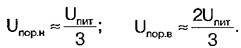
A typical circuit of an inverting comparator with voltage "hysteresis" is shown in fig. 3. The values of the lower and upper input threshold voltage Uthr.n and Uthr.v are determined by the following relationships:

Provided R1=R2=R3
Voltage values at the output of the comparator: U°=Us; U1 \u4d Upit - Iut RXNUMX. The saturation voltage Unas depends on the load current:

(Iut is the output leakage current; the current through the resistor R3 at high values of the resistance of the resistors R1-R3 can be ignored due to its smallness).

On fig. 4 shows a typical circuit of a non-inverting comparator with voltage hysteresis. For him

The transfer characteristics of the inverting and non-inverting voltage comparators described above are shown in fig. 5a and b, respectively.
It should be noted that in order to ensure stable threshold voltage values, it is necessary to power the comparator, both inverting and non-inverting, and especially the exemplary voltage driver (in Fig. 3 and 4 - resistive dividers R1R2) from a stabilized source.
Let's briefly consider several options for using the comparator.
On fig. 6 shows a diagram of a rectangular pulse generator. It is based on an inverting voltage comparator with "hysteresis" and has the same switching thresholds. Elements R4, VD2 form the charging circuit of the capacitor C1 and determine the duration of the output pulse τi=R4·C1·ln2. Through the elements R3, VD1, the capacitor C1 is discharged, forming a pause tn=R3·C1·ln2. The processes occurring in the generator circuits are illustrated in Fig. 7.

Due to the fact that the comparators have an open collector output, they can be connected in a wired OR circuit. To do this, it is enough to combine the outputs of the comparators (pin 1 and 7) and connect the output of the element to the positive power wire through a common load resistor with a resistance of 3 kOhm.
On fig. 8 shows a schematic of a zero crossing detector. The basis of the node is an inverting voltage comparator with "hysteresis". With the resistor values indicated in the diagram, the threshold levels given to the input correspond to: Uthr.n = -0,0023Upit; Uthr.v \u0,0027d 1Upit. At the output, the detector generates a short pulse each time the input voltage passes through "zero". Diode VDXNUMX protects the comparator from input current overload during negative half-cycles of the input signal.
Authors: M.Shapolvalova, A.Shestakov, N.Minina, Bryansk
 See other articles Section Reference materials.
Read and write useful comments on this article.
<< Back
 Latest news of science and technology, new electronics:
Traffic noise delays the growth of chicks
06.05.2024
The sounds that surround us in modern cities are becoming increasingly piercing. However, few people think about how this noise affects the animal world, especially such delicate creatures as chicks that have not yet hatched from their eggs. Recent research is shedding light on this issue, indicating serious consequences for their development and survival. Scientists have found that exposure of zebra diamondback chicks to traffic noise can cause serious disruption to their development. Experiments have shown that noise pollution can significantly delay their hatching, and those chicks that do emerge face a number of health-promoting problems. The researchers also found that the negative effects of noise pollution extend into the adult birds. Reduced chances of reproduction and decreased fertility indicate the long-term effects that traffic noise has on wildlife. The study results highlight the need ... >>
Wireless speaker Samsung Music Frame HW-LS60D
06.05.2024
In the world of modern audio technology, manufacturers strive not only for impeccable sound quality, but also for combining functionality with aesthetics. One of the latest innovative steps in this direction is the new Samsung Music Frame HW-LS60D wireless speaker system, presented at the 2024 World of Samsung event. The Samsung HW-LS60D is more than just a speaker system, it's the art of frame-style sound. The combination of a 6-speaker system with Dolby Atmos support and a stylish photo frame design makes this product the perfect addition to any interior. The new Samsung Music Frame features advanced technologies including Adaptive Audio that delivers clear dialogue at any volume level, and automatic room optimization for rich audio reproduction. With support for Spotify, Tidal Hi-Fi and Bluetooth 5.2 connections, as well as smart assistant integration, this speaker is ready to satisfy your ... >>
A New Way to Control and Manipulate Optical Signals
05.05.2024
The modern world of science and technology is developing rapidly, and every day new methods and technologies appear that open up new prospects for us in various fields. One such innovation is the development by German scientists of a new way to control optical signals, which could lead to significant progress in the field of photonics. Recent research has allowed German scientists to create a tunable waveplate inside a fused silica waveguide. This method, based on the use of a liquid crystal layer, allows one to effectively change the polarization of light passing through a waveguide. This technological breakthrough opens up new prospects for the development of compact and efficient photonic devices capable of processing large volumes of data. The electro-optical control of polarization provided by the new method could provide the basis for a new class of integrated photonic devices. This opens up great opportunities for ... >>
| Random news from the Archive Front cameras for smartphones 1080p, 60fps
11.05.2013
OmniVision Technologies has unveiled its new 1/6-inch image sensor for smartphones, ultrabooks and tablet computers OV2724. The main feature of integrated circuits was the ability to shoot high-resolution video at 60 frames per second. The novelty is positioned in the sector of "top" gadgets, and the main purpose of the sensors will be the use in front cameras for chats and conferences using mobile devices.
The OmniVision OV2724 sensors are based on the OmniBSI-2 architecture with 1,34 micron pixels. The devices work perfectly not only in "normal" conditions, but allow you to get high-quality video in difficult cases: with insufficient, and vice versa, excessive scene illumination.
In fact, this is still the best image sensor for front cameras from all that are on the market today. However, it will be possible to evaluate its advantages in business in six months or a year: today OmniVision supplies only engineering samples. OmniVision OV2724 integrated circuits will enter the series only in the third quarter of 2013.
|
Other interesting news:
▪ Handheld x-ray scanners
▪ The Milky Way is almost invisible
▪ Kevlar for battery
▪ The end of PANASONIC VCRs
▪ Lethal dose of chocolate calculated
News feed of science and technology, new electronics
 Interesting materials of the Free Technical Library:
▪ section of the site Personal transport: land, water, air. Article selection
▪ article And instead of a lamp, a plasma motor. video art
▪ article Who put their Rolls-Royce on the tracks to go hunting? Detailed answer
▪ article Car Kozlik. Personal transport
▪ article Christmas tree decoration New Year's electronic 5-beam asterisk with microprocessor control. Encyclopedia of radio electronics and electrical engineering
▪ article Refinement of the welding transformer TDE-101U2. Encyclopedia of radio electronics and electrical engineering
Leave your comment on this article:
 All languages of this page
Home page | Library | Articles | Website map | Site Reviews

www.diagram.com.ua
2000-2024


 Arabic
 Bengali
 Chinese
 English
 French
 German
 Hebrew
 Hindi
Hindi Italian
 Japanese
 Korean
 Malay
Malay Polish
 Portuguese
 Spanish
 Turkish
 Ukrainian
 Vietnamese