|
|


 Arabic
 Bengali
 Chinese
 English
 French
 German
 Hebrew
 Hindi
Hindi Italian
 Japanese
 Korean
 Malay
Malay Polish
 Portuguese
 Spanish
 Turkish
 Ukrainian
 Vietnamese
|
ENCYCLOPEDIA OF RADIO ELECTRONICS AND ELECTRICAL ENGINEERING Multi-channel amplification in UMZCH with extremely deep OOS. Encyclopedia of radio electronics and electrical engineering
Encyclopedia of radio electronics and electrical engineering / Transistor power amplifiers The author proposes an original multichannel structure of the transistor UMZCH. This amplifier achieves very low distortion due to multi-loop feedback. Wideband (up to 100 MHz) OOS is achieved in the low power main channel with very low delay. In fact, the author has developed a precision high-speed amplifier. Not least of all, the reason for writing the article was the ongoing debate among audiophiles about the dangers of OOS and the restriction of its use. Unfortunately, superficial impressions are more than enough to accuse the OOS of incorrectness. Of course, criticism of deep NOS is generally not serious; the reason for the negative result should be sought in the circuit design of the amplifiers. In receiver-amplifier devices for professional and military purposes at frequencies up to 1 GHz [1], it is recommended to use cascades with precisely NFB, as providing the maximum dynamic range and linearity. Similar recommendations are implemented in amateur radio equipment [2]. The fundamental criterion for the linearity of an "ideal" amplifier is the scale identity of the instantaneous values of the input and output signals. It is OOS that stabilizes the gain of the amplifier in terms of parameters determined by the structure and type of feedback. The quality of stabilization is determined by the gain margin inside the CNF loop [3]. Gain margin - over 120 dB in a 20 kHz band - commensurate with the dynamic range of the device, allows you to generate an output signal with an error of less than 0,0001%. Thus, the use of extremely deep feedback should be considered mandatory to ensure high-quality amplification of wideband signals and the linearity of transistor amplifiers. Unfortunately, despite the well-known terms of these concepts, they are often interpreted in a rather strange way or ignored altogether, so certain comments are required. Criteria and principles of environmental protection Many UMZCH developers pay attention to the fact that the amplifier must have high linearity even before the OOS coverage. However, it is most important that the UMZCH has a high linearity in the frequency range, the period of which is close to the time of signal passage through the amplification stages covered by the OOS. Since the feedback no longer works at these frequencies, nonlinearities and noise provoke the appearance of combination components in the process of parasitic modulation in the UMZCH cascades. In the frequency range where the NOS is still in effect, unpleasant effects are possible when the feedback efficiency is greatly reduced under certain conditions [4]. It turns out that the signal at the output of the amplifier is very similar to the input, but nevertheless contains a complex tangle of parasitic components. As a result of such amplification, phase multiplicative distortions appear, similar to the "jigger" in digital transmission channels. The basis of high linearity should be considered the operation of electronic devices in a low-signal [5], close to static mode, since changes in their electrical parameters under the influence of a signal or a destabilizing factor are the root cause of distortions. A large signal level leads to changes in the amplifying and time-frequency parameters of the cascades. The time for the signal to pass through the stages of the amplifier depends on many factors, which leads to the appearance of "jitter-like" phenomena, regardless of the presence of feedback. At the same time, for the FOS, it is fundamentally important that the feedback signal delay time is extremely short, which is actually close to the signal transit time through the amplifier cascades, because at this time the FOS signal is delayed relative to the input signal. The greater the level of this signal (i.e., the greater the gain) and the delay time of the signal, the greater the parasitic modulation and distortion. Accordingly, more stringent requirements are imposed on the overload capacity of the cascades. Overloading the cascades blocks the stabilizing functions of the environmental protection. The probability of overload is actually related to the response time * through the feedback loop (the time between the arrival of a signal at the input of the amplifier and its response back through the feedback circuit). Most of the shortcomings of UMZCH with deep OOS are connected precisely with forcing amplification at frequencies whose period is close to the time of signal passage through the amplification stages covered by OOS. The degradation of the amplifier quality progresses with an increase in the delay time in the feedback loop, aggravated with an increase in the number of stages. In other words, the number of successive amplification stages at a large depth of the total feedback is very limited. It should be noted that the use of transistor stages with a common emitter (including differential stages and current generators) has a very negative effect on both the modulation and overload characteristics of the amplifier. Cascades of this kind actually represent a mixer, where its dynamic range serves as a criterion for linearity. In the range of modes allowed for transistors, the upper limit of the dynamic range is proportional to the current through the mixer [2]. In other words, the cascades must have a large dynamic range and the corresponding current and voltage modes for transistors, and their changes in the presence of a signal are minimal. The signal itself must be sufficiently "slow" in comparison with the speed of the amplifying elements, then there is less signal change during the reaction time in the feedback loop and less distortion. The cutoff frequency Fgr of amplifying devices should be as large as possible the frequency of unity gain F1 of the amplifier. Thus, an extremely limited number of stages and an extremely short response time of the feedback loop are the fundamental conditions for achieving linearity in a wide band and a large dynamic range of the amplifier. Moreover, the cascades must operate in class A, and so that outside the operating band their transfer coefficient is significantly less than one. In other words, in the absence of "humps" in the frequency response, the closing frequency Fdet of the CNF loop (Fdet is the reciprocal of the response time of the FOS loop) should be much higher than the frequency of unity gain (Fdet >> F1), and the signal at frequencies close to Fdet should be greatly attenuated. At the same time, with an extremely deep OOS, a low level of penetration of the output signal to the UMZCH input at the frequency of closing the OOS loop should be simultaneously ensured. The last factor is very important, since it is in the UMZCH that the output signal level (in terms of voltage) is large, and the intermodulation efficiency has a dependence close to the cube of the input signal [2]. In turn, the general NF circuit should not have any additional (and parasitic) connections with intermediate UMZCH cascades or with local NF circuits. The meaning is simple: it is necessary to exclude the penetration of the pre-distorted signal into the loop of the general OOS. The gain with OOS enabled should be minimal. In other words, the lower the gain, the proportionally higher the signal-to-noise ratio + interference and the proportionally lower the unity gain frequency of the UMZCH at a fixed loop gain cutoff frequency. Note that an increase in the input signal level and the use of ultra-low noise input amplifiers can lead to a deterioration in the input overload characteristics of the UMZCH. The signal path circuits, as well as the input and OOS (especially at RF) must be relatively low-resistance (tens to hundreds of ohms). And here you should pay attention to the fact that a decrease in the resistance of the circuit that controls the transistor, connected according to the circuit with a common emitter (CE), sharply worsens its overload characteristics. Resistors in the base and emitter circuits of amplifying stage transistors significantly improve their linearity and overload characteristics. Increasing the input resistance reduces the input current and thus simply and effectively reduces the gain at frequencies close to F. In this case, it is highly desirable to turn on these resistors (to reduce the gain) in each amplification stage [4, 6], but the greatest efficiency is achieved when they are turned on precisely at the amplifier input [7]. These resistors perform similar functions in radio frequency devices [2] (amplifiers, mixers, etc.), reducing the amplification of the cascades at the cutoff frequency (Fgr = Fzam) of the transistors used and reducing their tendency to self-excitation. However, it should be noted here that with a large change in the base current, the resistor in the base circuit can create a very large level of distortion. As a consequence, the use of resistors in the base circuits should only be used when the transistor is operating in structures with very deep feedback. Finding a compromise among the mutually exclusive requirements listed above is often a thankless task. Absolute execution and combination of them in one amplifier is simply unrealistic. It is only possible to realize an extremely deep OOS, as well as the indicated requirements, only with multichannel amplification, i.e., on the basis of Multichannel Amplifying Structures (MCUS). Criteria and principles of the ICCC The use of MKUS makes it possible to radically reduce the signal delay time in the amplifier, i.e., to ensure an extremely short response time of the feedback loop. As a result, it becomes possible to sharply increase the frequency of closing the CNF loop (Fc), to provide a very large gain margin - and all this at a noise level close to the limit. In this version of the amplifier, it is possible to combine the advantages of various approaches in circuit engineering, using significantly different nodes with different specifics and often with unique characteristics. In such structures, it is possible to use different amplification classes (A, B, C and even D), switching circuits and types of electronic devices. The options for connecting additional amplification channels in this case are based on the criterion of suppressing the signal of the main channel (both at its input, output, and inside) by means of its additional amplification and transmission to the output circuit. In general, the process of transmitting this signal can be carried out by other amplifiers. Thus, it is possible to create a very large gain margin inside the CNF loop and thereby provide an extremely small error in the CNF loop. For the consequence of an ideal gain in an amplifier with a common OOS is ... the absence of a signal at the output of the adder of direct and return (along the OS circuit) signals. Here the concept of the main (main) amplifier (channel) expresses its priority in closing the feedback loop with a decisive influence on the formation of an undistorted output signal. The main parameter of the main amplification channel should be considered its delay time, which should be extremely small. Specific parameters of additional amplification channels can be the level of intrinsic noise, output power, etc. It should be noted that the principles of multichannel (parallel) signal processing have been known for a relatively long time [9], but, unfortunately, apart from precision measuring equipment, they are rarely and modestly used. Especially in the implementation of a large gain margin inside the OOS loop. At the same time, a number of schemes of both UMZCH [5, 10] ** and broadband op amps fall under the concept of MKUS. Thus, it is advisable to supplement different approaches in UMZCH circuitry [3-8] with the logic of parallel operation of amplifiers, i.e. MKUS. It should be noted that the number of options for building amplifiers based on MKUS is quite large, but in relation to UMZCH it makes sense to use structures that, due to a very large gain margin, would make even a powerful and often low-frequency output stage perform its functions flawlessly.
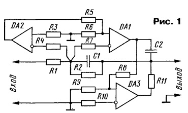
As an example of MKUS, consider the circuit (Fig. 1) of a three-channel inverting amplifier designed to operate on a low-power load. Here, op amp DA1 (appropriately adjusted) is the main channel of the amplifier that sets the closing frequency of the CFO loop (Fzam), and amplifiers DA2 and DA3 form additional channels that operate according to the criterion of signal suppression, respectively, at the input and output of DA1. So, the signal that came through the resistors R1, R7 to the input of the op-amp DA1 is amplified and through the capacitor C2 is fed to the output of the amplifier. Elements C1, R2 and R1 form an OOS loop. Additionally, the signal is amplified through the DA2 channel, as well as DA3, from which it passes to the common output through the resistor R11. Thus, in relation to low-frequency signals, the gain inside the CNF loop increases significantly. Signal dividers R5R6 and R8R9 provide priority to the main channel (DA1), reducing the gain of DA2 and DA3 to a level at which the additional phase shift introduced by these op-amps is easily compensated by the main channel. Here you should be guided by the rule: the signal should be reduced (divided) precisely at the input of additional amplification channels, which significantly improves their overload characteristics. An exception can only be amplifiers connected to the input (DA2), due to the deterioration of the signal-to-noise ratio. Resistors R4 and R7 improve input overload characteristics. Similar functions, albeit indirectly, are performed by the elements R3 and R10; they significantly reduce the gain of the input stages of the op-amp, especially near Fdet. It should be emphasized here that such resistors eliminate this problem, since the frequency correction of the op-amp according to the standard method, as a rule, does not protect the input stages of the op-amp from RF signal overload. In the absence of these resistors, high-frequency distortion products through the capacitor C1 go directly to the inputs of the op-amp and overload them (gain is forced at frequencies close to Fzam). In turn, deep OOS for RF (through capacitor C1) creates a large drop in the frequency response of the amplifier at the frequency F1 of the op-amp DA1. Thus, high overload characteristics are provided both at the DA1 output and at the DA3 input, and as a result, the entire amplifier as a whole. At audio frequencies, the signal is sequentially amplified by three op-amps - DA2, DA1, DA3 (they can also be made using MKUS technology). The use of an op-amp simplifies the implementation of the design, although the use of both high-frequency and microwave transistors is not forbidden. Turning to the UMZCH option, it is very tempting to use a powerful amplifier (hereinafter ULF) as DA3, with a high output resistance of which the resistor R11 could be excluded. Another solution is also possible: instead of elements C2 and R11, use a more efficient matching device (multichannel), then ULF can be made as a separate unit! This makes it possible to reduce the level of interference and interference by 20...40 dB. As for other amplifier units, here it is technologically expedient to use extremely broadband (radio frequency) op-amps that allow operation with one hundred percent OOS. In other words, the extremely short signal transit time and, accordingly, the minimum phase shift at the unity gain frequency are decisive parameters when choosing an op-amp. The whole range of arguments is quite complicated, and therefore the choice fell on a relatively average broadband op amp. Of course, the use of an ultra-modern element base with "sky-high" characteristics is quite impressive, but at a high price it is not advisable. Meanwhile, the high efficiency of the MKUS with the addition of signals at the output of the amplifier (with a high-quality matching device) makes it possible to use transistors with modest parameters in the output stage of the low-frequency channel. Due to the relatively low cut-off frequency Fgr of powerful bipolar devices, it is necessary to focus on the essential requirement discussed above: the operation of transistors near the frequency is not allowed and, as a result, the amplification of the UMZCH (with CNF turned on) at this frequency should be insignificant (F1 < Fgr). Increasing the cutoff frequency of the CFO loop to the ratio F1> Fgr leads to the fact that the input amplifier (usually very broadband) causes an overload of the subsequent low-frequency cascades of the UMZCH. Based on the principles outlined here, united by the MKUS technology, the author has developed a scheme for a relatively simple three-channel UMZCH, shown in Fig. 2. Its rated power Pout 75 W when operating on a load Rn = 4 ohms.
The main amplification channel (DA1, VT1) uses an AD812 RF op-amp. Its unity gain frequency F1 = 100 MHz, self-noise EMF Esh = 4 nV/Hz, and the gain is about 40 dB at a frequency of 3 MHz, corresponding to the frequency Frp of powerful ULF transistors (A1 in Fig. 2), which allows you to effectively suppress distortion of the ULF output stage. It is the main channel that determines the closing frequency of the CNF loop (Fzap and the stability of the UMZCH at frequencies above Fgr. A very short and stable reaction time of the CFO loop is ensured by the speed of the main channel and the operation of the repeater on VT1 in class A mode, which eliminates jitter-like phenomena (phase modulation). In this scheme, the main channel operates in the band from audio frequencies to the frequency Fzam. The specificity and priority of the main channel is its operation at frequencies close to Fzam, and the closing of the OOS loop. Let us consider the operation of the UMZCH in the frequency band from F1 = Frp = 3 MHz to Fdet = 250 MHz, using a pulsed signal with steep fronts for analysis. The input signal through resistors R1, R2 comes to the UMZCH signal input (point A), then through resistor R9 - to the input of the op-amp DAI, VT1, the emitter of which is the output of the main channel (point B). From the output of the main channel through the elements C7, C8 and R22 of the matching device, the signal passes to the UMZCH output (point C), where this signal dominates the signal that came from the ULF, and then through the C2 circuit, R3 closes the OOS circuit to the UMZCH signal input at point A. The low-resistance RF OOS circuit (elements C1, C2, R2, R3) provides high-quality division of the signal at these frequencies, while inductance L1 and T1 separate parasitic (mounting) capacitances. The signal operating at point A is additionally amplified by the second (DA2) amplification channel. This additional amplification channel is enabled by the criterion of main channel signal suppression (DA1) at its input. For a signal, the channel on DA2 is a preamplifier; it "turns off" only at the highest frequencies (above 10 MHz), where a phase shift that is unacceptable under stability conditions occurs. The amplified op-amp DA2 signal through the DA1 priority device (signal divider R10R11) is fed to the non-inverting input DA1. At audio frequencies, the DA2 output has a very low signal level, i.e. it works almost in a static mode. Thus, the signal amplified in series by two op amps (DA2, DA1) also comes to the output of the main amplification channel (point B). There, the signal branches off through the resistor R23 to the third amplification channel - A1 (ULF), from the output of which the signal of the audio and "zero" frequency through the matching device (secondary winding of the transformer T1) comes to the output of the UMZCH (point C). At frequencies where the speed of the ULF is limited, the output stage on VT2 with the transformer T1 works according to the criterion for suppressing the amplitude and phase errors at the output of the ULF. The use of inductance in the form of T1 is dictated by the need to fulfill two conflicting conditions: a very low resistance of the matching device at audio frequencies and high at frequencies close to Fgr, powerful transistors. It should be emphasized here that the issue of correct matching of low-resistance RF and LF structures is very important due to the occurrence of various parasitic resonances. In this case, the resonance occurs in a circuit consisting of a capacitor C7 and the inductance of the secondary winding T1, and is closely related to the gain and phase at the ULF output. Circuit C8, R22 reduces the frequency and quality factor of this circuit. The oscillatory circuit of the elements C9, R27 and the inductance of the primary winding of the transformer T1 reduce them even lower, as they are tuned to an even lower frequency. The transformer should be considered as a filter (LPF) and as an element of the signal adder at the UMZCH output, which suppresses the remnants of parasitic resonant manifestations and phase error using the amplifying resources of the main channel on DA1. The primary winding T1 is connected to an emitter follower on a transistor VT2, which at the same time is a current stabilizer for VT1. The priority of the main channel (DA1) is provided if the transformer is step-down. The voltage of the secondary winding T1 is actually switched on in series with the voltage coming from the ULF output. To effectively suppress ULF distortion, the transformer must be sufficiently broadband, have high efficiency (good flux linkage) at frequencies of the order of Fgr. RF microcircuits need to be powered by a separate bipolar regulator with a voltage of ±12,5 V. Now about the ULF, the scheme of which is shown in Fig. 3. Its output stage is a powerful symmetrical emitter follower controlled by a current generator [8]; the scheme is classic and does not need comments. ULF is enabled according to the criterion of signal suppression at the output of the main channel. Before the ULF, a device for creating the priority of the main channel (DA1) is included - a divider of resistors R23 (see Fig. 2) and R32 (Fig. 3). Its task is to reduce the ULF gain at frequencies around Fgr with a minimum phase change, and at higher frequencies, to reduce the gain to zero by means of C20. This improves the overload characteristics and noise immunity of the ULF.
So, the contribution of the ULF to the output signal of the UMZCH at high frequencies (above 3 MHz) decreases three times: as a result of deep OOS (due to the decrease in the frequency response at frequencies Fgr), the divider R23R32 and C20, and also due to the high inductive resistance of the winding T1. At a frequency of about 15 MHz, the voltage at the ULF output (at point E) is 180 ° behind the voltage at the UMZCH output (at point C)! Capacitor C25 in the ULF performs a dual function. In addition to creating a ULF frequency correction, in a cascade on transistors VT6, VT7 it forms a parallel channel at frequencies above 3 MHz. The signal from the VT3 emitter is fed through the capacitor C25 (bypassing VT4 and VT7) to the output emitter followers (with the ULF input level), reducing the signal transit time through the ULF. Here it is necessary to point out the ambiguous role of the lead correction circuit by means of capacitor C22. This capacitor reduces the phase shift of the signal at the ULF output (at frequencies of the order of 3 MHz), while the signal level at the output of the main channel decreases (point B). But the capacitor C22 boosts amplification at frequencies above Fgr, which worsens the overload characteristics of the channel and increases its distortion. Therefore, the use of C22 is justified only when using insufficiently high-frequency transistors (series KT818, KT819); in other cases, the chain R34, C22 should be excluded. Thus, the signal at the output of the UMZCH (point C) is actually a composite one. Signals in the operating frequency band pass to the output from the ULF through the secondary winding T1. and the compensation signal for suppressing ULF distortion at high frequencies is through transistors VT1, VT2 and transformer T1. The sequential gain of all channels (DA2 DA1, ULF) at a frequency of 20 kHz reaches 160 dB. which reduces the error with the introduced FOS to a value of less than 0,0001%. The smallness of this error (signal level at point A) can be visually assessed after its amplification by the RF op-amp DA2 (at point D), using the method of I. T. Akulinichev [3] known to the readers of the journal. But due to the huge gain margin inside the feedback loop, the error is very small (less than 1 mV) and it is almost linear. However, here you need to pay attention to the level of interference and parasitic connections in the signal circuits, including through common wires. For example, the current in the OOS circuit (through elements C1, C2, R2 - R5) at a frequency of 20 kHz creates a voltage drop on the SCR wire at a level of several microvolts with respect to the precision circuit OP1. This pickup on the SCR is linear and does not pose any danger. But despite the scantiness, the pickup, amplified thousands of times, significantly increases the signal level at the output of the op-amp DA2. To correctly observe the magnitude of the error in the CNF circuit, one common wire should be used for all stages, by closing OP1-OP4 to OP5, and an additional amplifier by 20 ... 40 dB. Oscillograms of a sinusoidal signal with a frequency of 20 kHz are shown in fig. 4 during operation of UMZCH with output power Pout = 75 W; from top to bottom: output DA2 (point D) at a scale division of 1 mV, output DA1 (point B) - at a scale division of 0,5 V. High-frequency interference at the input of the amplifier is attenuated by the R1C1 filter, and its capacitor is also included in the RF OOS circuit (R2 / R3 \u2d C1 / C7). The low-resistance OOS circuit drastically reduces the effect of RF interference and parasitic capacitances. Resistors R9 and RXNUMX effectively increase the overload capacity of RF op amps, significantly reducing the RF gain of their input stages. The combination of these measures significantly reduces intra-loop amplification at frequencies close to frequencies, excluding ULF amplification at the cutoff frequency of powerful transistors, which ensures high overload characteristics. At frequencies below 200 kHz, the gain is determined by the ratio (R3+R4+R5)/(R1+R2) =10. Transistors VT8, VT9 stabilize the quiescent current of the output stage [3] according to the criterion of stabilization of the bias voltage at the bases of the output transistors. In case of current overload, the transistors VT5 and VT20-VT22 block the ULF (VT10-VT19) for eight cycles of the generator, made on the elements DD1 1-DD1 3 (i.e., for about 30 ms).
Control and tuning of the UMZCH should be carried out in a band of 100 MHz. To do this, it is advisable to increase the cutoff frequency of the OOS loop by halving the resistance of resistors R1 and R4 + R5. After, by turning off DA2 (for this it is enough to unsolder one of the conclusions of R10), at point C they control the monotonous decline in its frequency response at frequencies above 1 MHz. If necessary, the gain of the main channel DA1 is reduced by increasing the resistance R9. Then, a meander pulse signal with a frequency of 250 kHz with a voltage swing of 0,5 V is applied to the input. There is no point in supplying a higher signal level, since the output power of the UMZCH at frequencies above 250 kHz is strongly linked to the power of the output stage of the main amplification channel (VT1, VT2). In this case, the predistorted signal from the DA1 output (point B) should be considered the most informative, which, in fact, is a multiply amplified signal of the OOS tracking loop error. The signal at point B should have an impulse character with a shape close to the exponent. With the correct setting, the pulses should be relatively short, their fronts should be steep, and the declines should be gentle and smooth. In no case should any resonances or breaks be observed on their oscillograms. Pulse signals at different points of the UMZCH, measured at a double cutoff frequency, are shown in the oscillograms of Fig. 5, when working on a resistive load with a resistance of 4 ohms - on the oscillograms of fig. 6; when working on a reactive load (capacitor with a capacity of 1 μF) - on the oscillograms of Fig. 7. Accordingly, from top to bottom: DA2 output (point D) at a division value of 0,2 V, DA1 output (point B) at a division value of 2 V, UMZCH output (point C) and ULF output (point E) at a division value of 5 V. The sweep rate for these oscillograms is 1 μs.
If necessary, first of all, the amplification and correction of the ULF (elements R35, R34, C22, C25), the signal attenuation coefficient of the priority device (R23, R32, C20, C21) are first adjusted, and then the matching device is adjusted (C7, C8 and R22, C9 and R27, T1), excluding the oscillatory process of establishing a signal at the output of DA1 (point B). Next, connect and select the resistor R10 according to the criterion of the minimum amplitude of the pulses at the output of DA2 with a high linearity (smoothness) of the latter. After that, the denomination is chosen by 10 ... 20% more and soldered onto the board. The quiescent current of the ULF output stage is regulated at a level of about 100 mA by selecting resistor R48, the ULF blocking current (8 A) is R63, and the quiescent current of the transistor VT1 (200 mA) is R25, respectively. And finally, the operation of the UMZCH is checked for the absence of ULF excitation when overloaded with a large input signal in the band of 30 ... 300 kHz. The excitation of the ULF indicates its very low speed and overload properties, a large gain on F^, an excessively high cutoff frequency of the NF loop or insufficient priority of the main channel, which is possible when the components change. After tuning, the cutoff frequency of the CNF loop is restored. Construction and details It is the main channel that determines the delay time of the OOS tracking loop, the gain at high frequencies and, as a result, the effectiveness of suppressing various kinds of parasitic resonances and distortions. Thus, the most stringent requirements are imposed on DA1: it must be radio frequency, i.e., it must work correctly with a high level of RF signal and with a standard load of 50 ohms. High demands are also placed on the transistor VT1, which also introduces a time delay. Therefore, it must be high-frequency (for example, from the KT922, KT925 series), and its current is sufficient to work with the op-amp DA1. Due to the relatively small current VT1 (200 mA), the UMZCH load impedance at frequencies above 1 MHz must be greater, and the presence of a filter (inductor L1) is mandatory. Another purpose of L1 is to block the passage of high-frequency oscillations from the AC to the UMZCH output (to point C) and further to the OOS circuit. Due to the very high frequency of closing the CNF loop, the physical length of the main amplification channel and the CNF circuit on the RF should be minimal, and the implementation should take into account the requirements for RF devices. The requirements for the op amp DA2 are less stringent, but it should be emphasized that it is the op amp DA2 that is the preamplifier that determines the level of noise, interference, the precision of the OOS, etc. as a consequence, he is obliged to work in "greenhouse" conditions. The conditions are as follows: the presence of a relatively high-resistance resistor in the input circuit (R7), which eliminates the overload of the op-amp at frequencies close to the frequency Fzam; operation of the output stage of the op-amp in the low-signal mode of class A; the presence of a separate power supply or RC filters in the power circuits to reduce interference. In the design, it is important to have separate common wires: signal OP1 and power circuit OP2. "The question of the "ground" is very important, because the signal in the stages of the amplifier is determined in relation to the common wire [8]. The induction of low-frequency interference on the signal part or the signal common wire is actually identical. Therefore, the OP1-OP4 circuits must be in the screen (aka the OP5 wire) and must be made with separate wires. The cascade on the op-amp DA2 should also be shielded. ZCH. High requirements are placed on the quality of the capacitor C2, since the entire ULF output voltage is applied to it. Therefore, it must have low absorption and a rated voltage of at least 250 V (from non-deficient ones - KSO, SGM); capacitor C1 is desirable to use the same group. Input circuit resistors and OOS (R1-R5) - MLT or OMLT. Capacitors C7-C9 in the matching device - K73-17 or ceramic with a small TKE. It should be noted that to exclude excitation, transistors VT8, VT9 must be located in close proximity to VT6, VT7 and VT10-VT13. When the amplifier is excited, it is recommended to double the resistances of resistors R47-R49 and R51, R53 or apply a bias similar to that used in [4]. There are no other requirements for the ULF element base, therefore, its implementation based on other schemes is possible. However, preference should be given to more advanced (i.e., broadband and multichannel!) circuitry and element base, in no case should the gain be forced due to its overload characteristics. It is permissible to increase the output power of the UMZCH without changing the circuit up to 120 W by using transistors KT14, KT9 in the VT8101-VTT8102 cascade and increasing the collector current VT1 to 250 mA. As mentioned above, ULF can be removed from the main UMZCH channel at a distance of up to 40 cm (with the indicated component values). For the author, with a breadboard version, the length of the wires from the resistor R23 and from the transformer T1 to the ULF is 30 cm. Conversely, the length of the conductors from the emitter VT1 to R23 and from the elements C7, R22 to the transformer T1 should be minimal. Coils LI, L2 are wound on a frame with a diameter of 12 mm and contain 11 turns of SEW wire with a diameter of 1 mm. Transformer T1 is wound on the same frame. The primary winding contains 30 turns of PEV 0,3, the secondary - 15 PEV 1 mm. It is advisable to wind the primary winding with a double wire over the secondary between its turns. It is even better to wind the transformer with a bundle of 10-12 PEV wires 0,3 ... 0.4 mm, two of which, connected in series, form the primary winding (30 turns), and the remaining wires connected in parallel form the secondary winding (15 turns). Of course, a high-quality UMZCH should have an indication of the overload of the amplifier in terms of current and voltage, a device for stabilizing the "zero" at the output of the UMZCH, compensation for wire resistance, and speaker protection [4, 8]. In conclusion, the author would like to thank A. Sitak (RK9UC) for his help in preparing this article. Literature
Author: A.Litavrin, Berezovsky, Kemerovo Region
Machine for thinning flowers in gardens
02.05.2024 Advanced Infrared Microscope
02.05.2024 Air trap for insects
01.05.2024
▪ HP Metal Jet technology for 3D metal printing ▪ The world's largest Cherenkov telescope launched ▪ Updated Specification for Lightning Connector
▪ site section Parameters, analogues, marking of radio components. Article selection ▪ article Paris is worth a mass. Popular expression ▪ article Why do we cry? Detailed answer ▪ article Small-fruited double crest. Legends, cultivation, methods of application
Home page | Library | Articles | Website map | Site Reviews
www.diagram.com.ua |


 Leave your comment on this article: