|
|


 Arabic
 Bengali
 Chinese
 English
 French
 German
 Hebrew
 Hindi
Hindi Italian
 Japanese
 Korean
 Malay
Malay Polish
 Portuguese
 Spanish
 Turkish
 Ukrainian
 Vietnamese
|
ENCYCLOPEDIA OF RADIO ELECTRONICS AND ELECTRICAL ENGINEERING Super-linear UMZCH with deep environmental protection. Encyclopedia of radio electronics and electrical engineering
Encyclopedia of radio electronics and electrical engineering / Transistor power amplifiers Is it possible to create an amplifier using domestic components that would successfully compete with any branded one? The author of the published article answered this question in the affirmative. Moreover, in UMZCH he used bipolar transistors and operational amplifiers. On domestic components, this ultra-linear amplifier with deep and broadband feedback provides long-term power up to 150 watts into a 4 ohm load. Using imported components, you can increase the power in an 8 ohm load up to 250 watts. It is able to work on a complex load, has input and output overload protection. UMZCH intermodulation distortion is so small that the author was forced to measure them at radio frequencies. The design and printed circuit board developed by the author is a sample for teaching the "wiring" installation of broadband devices. Some time ago, among audiophiles and radio amateurs, the opinion prevailed that a truly high-quality UMZCH must be made on lamps. Many arguments have been put forward as justification. However, if we discard the completely far-fetched ones, then only two will remain. First, the distortion introduced by a tube amplifier is pleasing to the ear. Secondly, the non-linearities in tube amplifiers are more "smooth" and produce significantly less intermodulation products. It must be said that both the one and the other are confirmed by practice. Moreover, there has long been even a special sound processing device - an exciter, the action of which is based precisely on the introduction of even-order distortions into the high-frequency part of the spectrum. In some cases, the use of an exciter makes it possible to improve the development of instruments and voices of the second or third plan, to give additional depth to the sound stage. A similar effect in an amplifier can be pleasant, sometimes even useful. Nevertheless, the introduction of "good-sounding" distortions is still more the prerogative of the sound engineer than the UMZCH itself. As for achieving fidelity of sound reproduction, from this point of view it is necessary to achieve the elimination of distortions introduced by amplifiers and loudspeakers. The topic of reducing the distortion introduced by loudspeakers was previously discussed in the article [1]. Here we will focus on the "classic" UMZCH with a low output impedance, since they are still more versatile than UMZCH with a "current" output. At first glance, it may seem that with today's state of the art, designing an amplifier "transparent" is not difficult at all, and the debate around this problem is just the fruit of advertising hype. In part, this is true: if you organize the mass production of an impeccable UMZCH, then after a while the industry that produces these amplifiers, in my opinion, will simply remain without sales. The author of these lines had to develop tube and transistor precision amplifiers for measuring equipment, repair and adjust various equipment - mostly foreign-made. Naturally, parameters were measured and structures were evaluated. And not only by standard (for audio equipment) methods, but also by more informative ones, in particular, by analyzing the spectrum of the output signal with a multi-tone input signal. (In this case, a signal is fed to the amplifier input, consisting of a sum of sinusoids of approximately equal amplitude with proportional to some set of coprime, i.e., not having common factors, numbers.) A similar technique is widely used to control amplifiers used in long-distance cable communication technology, since the requirements for the "non-pollution" of the spectrum of the signal passing through them are very stringent (thousands of such amplifiers are connected in series in the communication line, and their distortions are summed up). As an example, the amplifiers for the K-10800 system have an intermodulation distortion level of less than -110 dB in a frequency band of about 60 MHz. It is clear that obtaining such characteristics is not easy: the qualifications of the developers of such amplifiers must be very high. Unfortunately, audio manufacturers seem to be content with less skilled designers, with the possible exception of Rupert Neve, the designer of Neve and Amek sound recording consoles. I note that the latest Niva console (9098i), which received an enthusiastic assessment of recording professionals, is entirely solid-state, and its amplifiers have a very large depth of feedback. It is noteworthy that at one time Neave developed many lamp consoles, most of which were considered reference. Thus, having food for comparison and being a meticulous person, the author came to the conclusion that in many cases the actual quality of the work of most semiconductor, and even tube UMZCH, turns out to be much worse than follows from the measurement results using standard methods for audio equipment. It is known that many of them were adopted under the pressure of commercial circumstances and are very far from the realities of life. A good example is the list of requirements for the noise measurement method presented by R. Dolby in his article describing the CCIR/ARM2K methodology he proposed. The second item in this list is "...commercial acceptability: no manufacturer will use a new technique if the figures obtained from the measurement are worse than using existing ones ...". R. Dolby's proposed replacement of the peak meter by the average-rectified value meter improved the parameters by about 6 dB, and a twofold reduction in the weighting filter gain resulted in a total "gain" of 12 dB. Not surprisingly, this technique has been warmly received by many manufacturers. A similar "trick" is often made when measuring non-linear distortions: the entry made in the amplifier passport - "0,005% THD in the frequency range 20 Hz - 20 kHz" most often means only that the harmonics of a signal with a frequency of 1 kHz falling into the mentioned bandwidth should not exceed the specified value, but it does not say anything about distortion at a frequency of, say, 15 kHz. Some manufacturers believe that it is completely optional to connect the load to the amplifier when measuring distortion, while in the passport they indicate in small print: "... at an output voltage corresponding to the power of XX watts at a load of 4 Ohms ...". It is also not uncommon for an amplifier with a specification of "less than 0,01% THD" at a frequency of 1 kHz, working on a real load (with cables and speakers), to show intermodulation distortion according to the very gentle SMPTE standard (Two sinusoidal signal with frequencies of 60 Hz and 7 kHz, the ratio of their amplitudes is 4:1, and the measurement result is the relative value of the modulation of the amplitude of the high-frequency signal - low-frequency.) at the level of 0,4 ... 1%, and sometimes more. In other words, intermodulation distortion already at moderately high frequencies when working on a real load is much higher than the notorious harmonic coefficient. A similar phenomenon is also characteristic of many lamp UMZCH covered by voltage feedback. When analyzing the spectrum of a multi-tone signal amplified by such an amplifier, many combinational components are found. Their number and total power with an increase in the number of components of the input signal increase almost according to the factorial law, that is, very quickly. When playing music by ear, this is perceived as a "dirty", "opaque" sound, commonly referred to as "transistor". In addition, the dependence of the level of distortion on the signal level is not always monotonous. It happens that when the level of the useful signal decreases, the power of the distortion products does not decrease. It is clear that in such devices the passport set of amplifier characteristics (harmonic coefficient, frequency band) does not indicate anything other than the manufacturer's resourcefulness. As a result, an ordinary consumer often finds himself in a state of being a "pig in a poke" buyer, since he somehow fails to listen normally (with comparison in contrast) before buying. Of course, not everything is so gloomy - with regard to the color of the case, dimensions and weight, almost all companies that value their brand behave flawlessly. This in no way means that there are no UMZCH worthy of attention on the market at all - there are few of them, but they exist. Of all the industrial amplifiers with which the author had a chance to work, the old "Yamaha M-2" seemed to be the most "accurate" (they don't do anything like that in Japan now). Its price, however, is considerable, and it is not designed for a load of 4 Ohms, in addition, the output transistors in it work in violation of the requirements of technical specifications. From the amateur ones, the amplifier of A. Vitushkin and V. Telesnin left a very good impression [2]. It works clearly better ("transparent") than UMZCH VV [3]. Another good amplifier is M. Alexander from PMI [4]. Nevertheless, all these amplifiers do not fully realize the capabilities of the element base in terms of the real level of distortion, speed and reproducibility. For these reasons, as well as for reasons of engineering prestige, the author of this article preferred to develop his own version of the UMZCH, which would reflect the real capabilities of the element base (including those available in Russia and the CIS) and would be easy to repeat. At the same time, a "commercial" version was also developed using an imported element base - with even greater capabilities and greater output power. The main goal of the development was not so much to achieve high "passport" characteristics, but to ensure the highest possible quality in real operating conditions. Exceptional parameter values were obtained automatically as a result of circuit and design optimization. The main feature of the proposed UMZCH is the broadband achieved by a number of circuitry and design measures. This made it possible to obtain a unity gain frequency in the OOS loop of about 6 ... 7 MHz, which is an order of magnitude higher than in most other UMZCH designs. As a result, the achievable FOS depth in the entire audio frequency band is more than 85 dB (at a frequency of 25 kHz), at a frequency of 100 kHz the FOS depth is 58 dB and at a frequency of 500 kHz - 30 dB. The full power bandwidth exceeds 600kHz (at approx. 1% distortion). Below are the main characteristics of the UMZCH (when measuring distortion and slew rate, the input filter and the soft limiter are disabled).
The amplifier (Fig. 1) consists of the following components: a second-order input low-pass filter with a cutoff frequency of 48 kHz, a “soft” signal level limiter, the power amplifier itself, an output LRC circuit, as well as cascades for automatic DC balancing and wire resistance compensation ( four-wire load connection diagram). In addition, an auxiliary signal amplifier is provided at the UMZCH summing point. The appearance of a noticeable voltage at the inverting input of the amplifier, covered by parallel feedback, indicates a violation of tracking in the feedback loop and, accordingly, distortion, whatever the reasons they may be caused. This additional amplifier amplifies the distortion signal to the level necessary for the distortion indicator to work.
The signal path of the amplifier uses KR140UD1101 op amps, which are rarely used in audio equipment, but which, despite the age of development (Bob Dobkin developed his prototype LM118/218/318 back in the early 70s), have a unique combination of characteristics. So, the overload capacity for a differential input signal for K (R) 140UD11 (01) is 40 times better than for traditional "sound" op-amps. At the same time, it has excellent slew rate and gain per band (50x106 Hz at 100 kHz). In addition, this op-amp recovers from overloads very quickly, and its output stage operates with a large quiescent current and has high linearity even before feedback coverage. Its only drawback is that the EMF noise spectral density of this op-amp is about four times higher than the average for low-noise devices. In UMZCH, however, this does not matter much, since the maximum signal-to-noise ratio is no worse than 110 dB, which is quite sufficient for a given power. In the signal path, op-amps are used in an inverting connection to eliminate distortion caused by the presence of a common-mode voltage at the inputs. The power amplifier itself is built according to an improved "classical" structure [3, 5] - an op amp is connected at the input to ensure high accuracy, then a symmetrical voltage amplifier based on a "broken cascode" and an output stage based on a three-stage emitter follower follow. Due to seemingly minor improvements and design measures (Fig. 2), the real sound quality and reproducibility of the parameters of this amplifier are radically improved compared to [3, 5, 6].
The output stage, designed for a load of 4 ohms, uses at least eight transistors per arm. Despite the apparent redundancy and cumbersomeness, such a solution is absolutely necessary when working on a real complex load for two reasons. The first, and most important, is that when operating on a complex load, the instantaneous power allocated to the output transistors increases sharply. On fig. Figure 3 shows the dependences of the instantaneous power dissipated on the output transistors on the instantaneous value of the output voltage for different loads (curves 1-3) at a supply voltage of +40 V. Curve 1 corresponds to the operation of the PA on a purely active load with a resistance of 0,8 of the nominal (i.e. 3,2 Ohm), curve 2 - for a complex load with an impedance modulus of 0,8 of the nominal and a phase angle of 45 degrees. (requirement OST.4.GO.203.001-75), and curve 3 - at a phase angle of 60 deg. It can be seen from the graphs that when operating on a complex load, the peak power dissipated by the output transistors turns out to be 2,5 - 3 times greater than with a resistive load of the same modulus. This in itself is a problem, but the most troublesome fact is that the maximum power dissipated by the transistors when operating on a complex load occurs at times when the output voltage is close to zero, i.e. when a large power supply voltage is applied to the transistors. The impedance modulus of some loudspeakers can drop from 4 to 1,6 ohms (in a certain frequency band), and the phase angle can increase up to 60 degrees. [7]. This doubles the power dissipation compared to curve 3. For bipolar transistors, it is very important at what voltage power is dissipated on them: with an increase in voltage, the allowable dissipation power is significantly reduced due to the appearance of "hot spots" caused by local thermal instability, leading to degradation of parameters and secondary breakdown. Therefore, for each type of transistors, there is a safe mode area (OBR), within which their operation is allowed. So, for KT818G1 / 819G1 (they have the best OBR among domestic powerful complementary transistors), the maximum dissipation power at a voltage of 40 V and a case temperature of 60 ... 70 ° C is not 60, but 40 W, at a voltage of 60 V, the allowable dissipation power drops up to 32 W, and at a voltage of 80 V - up to 26 W. For clarity, in Fig. Figure 3 shows curve 4 showing the power dissipation capabilities of these transistors as a function of the amplifier output voltage. It can be seen that even when working on a purely active load, it is necessary to connect in parallel at least two devices per arm. Power field-effect transistors (MOSFETs, MOSFETs) have a higher OBR, but the degree of their complementarity is much worse than that of bipolar ones. This leads to the fact that the distortion of the MOS-FET output stage at low signal levels (due to the spread of the threshold voltage, as well as a larger output resistance) and high frequencies (due to the strong asymmetry of capacitances and transconductance) are several times greater than in a properly designed bipolar transistor cascade. Nevertheless, UMZCH with an output stage made on a MOSFET turns out to be cheaper in production abroad than on bipolar ones. The reason is that the prices for powerful bipolar and field-effect transistors abroad are approximately the same, and field-effect transistors require less. The OBR of the best imported bipolar transistors is significantly larger than that of domestic ones, however, when operating at a load of 4 ohms, they also need to be connected in parallel.
It is impossible to count on the short duration of power release, since the time of formation of current spots is measured in tens of microseconds, which is much less than the low-frequency half-cycle. Therefore, the number of output transistors must be chosen based on ensuring the operation of each of them within the boundaries of the OBR for direct current. This leads to the need to increase the number of output transistors, which is expensive and time consuming. This is why most commercial amplifiers have substantially fewer transistors than required. However, the parameters of transistors operated in violation of the OBR gradually degrade, which leads to a deterioration in sound. The second reason for the need for a large number of output transistors is related to the fact that their characteristics, primarily speed, begin to deteriorate with increasing current long before the maximum allowable currents are reached. So, for the widespread Japanese transistor 2SA1302, formally designed for 15 A, a sharp drop in the cutoff frequency starts from 3 A, and for its complementary 2SC3281, from 2,5 A. There are other reasons leading to the expediency of connecting several powerful transistors in parallel. An increase in the total capacitance of the base-emitter leads to the direct passage of the signal from the previous stage (with a certain power margin) and the bandwidth of the output follower actually exceeds the cutoff frequency of the output transistors. That is why in this amplifier it turned out to be possible to use relatively "slow" output transistors without compromising the achieved characteristics. The amplifier uses the element base of domestic production. In the signal path of each channel, OA K (R) 140UD1101 (3 pcs.), In auxiliary circuits - K (R) 140UD14 (08) and KR140UD23 (1 pc. each). Complementary transistors of the KT3102 and KT3107 series (2 pcs each), KT632 and KT638 (4 pcs each), KT502 and KT503 (2 and 1 pcs.), KT9115 and KT969 (3 pcs each) were used in the preliminary stages. KT961A and KT639E (4 and 5 pieces), as well as KT818G1 and KT819G1 (eight transistors per arm) are installed in the stages of the output stage of the amplifier. The amplifier also uses diodes of the KD521 or KD522, KD243B and KD213B series. On fig. 4 shows a schematic diagram of the UMZCH. The input low-pass filter is made on the op-amp (DA1) in an inverting connection. The signal from the low-pass filter output passes through a "soft clipper" implemented on VT1-VT4 transistors and VD3-VD14 diodes, and then goes to the input stage of the power amplifier itself, made on the op-amp DA3. It is followed by a symmetrical cascode transistor voltage amplifier on VT5-VT8, VT13-VT15 and a current amplifier (output follower) on transistors VT16-VT45. Op-amp DA2 performs the function of a signal amplifier at the UMZCH summing point for the operation of the distortion indicator.
The voltage amplifier following the op-amp DA3 has a high linearity due to the symmetry of the structure and a very deep (more than 40 dB) local OOS. The circuits of this OOS, together with R71C46 and DA3, are also used to form the required frequency response of the UMZCH loop gain as a whole. There is one subtlety in such a cascade: to minimize gain losses, the voltage drop across the resistors in the emitter circuits of the last cascode transistors (in Fig. 4 these are R59, R63) must be at least 2,5 V, or these resistors should be replaced with current sources . Otherwise, the linearity of the voltage amplifier deteriorates. Note that in the UMZCH described in [5] and especially in [3], this condition is not satisfied. In order to further increase the linearity (especially at high frequencies), the amplifier supply voltage is chosen to be 10 ... 12 V higher than the output stage supply voltage. Diodes VD17-VD19 are designed to accelerate transients when the amplifier exits from overload, as well as to protect the emitter junctions of VT5-VT8 transistors from degradation. Circuits R64C41, R66C42 exclude parasitic self-excitation VT13 and VT14, and diodes VD26, VD27 prevent saturation of the output stage transistors (these diodes must withstand a reverse voltage of at least 100 V at a current of 10 μA; most instances of KD521A or 1N4148 satisfy this condition). An unusual parallel connection of transistors in the first two stages of the follower provides effective equalization of currents through transistors, eliminating the need for their selection. Capacitors C45, C47-C49 prevent the occurrence of dynamic asymmetry in the output stage. The Zener diode VD25 delays the switching on of the transistors VT13 and VT14 during the charging of the storage capacitors of the power source, so that by the time they are turned on, the supply voltage of the op-amp reaches +5 ... 7 V and they enter normal mode. This measure prevents output voltage spikes when the power is turned on. For the same purpose, the auto-zero range at the UMZCH output is limited to +0,7 V. It may seem unusual to connect resistors in series in OOS circuits (R23, R24, R27C17 and R28C18 circuits, as well as R45, R46). This is done in order to reduce the non-linearity of the OOS circuits (the resistance values of the resistors and the capacitance of the capacitors, although to a very small extent, depend on the voltage applied to them). For the same reason, resistors R23, R24, as well as R122 and R123 are chosen with a large margin for dissipation power. Among other noteworthy features, it should be noted the initial bias device for the base of a three-stage follower, built on VT15 (it is mounted on a radiator of output transistors) and resistors R60-R62 and R65. The temperature coefficient of the bias voltage is chosen somewhat larger than usual to take into account the difference in temperature between the heatsink and the power transistor crystals. It is not quite common to use a capacitor C40. The absence of this detail in most designs leads to a dynamic change in the bias voltage and an increase in the nonlinearity of the amplifiers on signals with a rise or fall rate of more than 0,2 ... 0,5 V / μs. And this has a very significant effect on the magnitude of intermodulation distortion in the region of higher frequencies. By the way, the use of a "slow" transistor (such as KT15 or KT502) as VT209 prevents another often occurring, but rarely noticed defect - self-excitation of the transistor at frequencies of the order of 50 ... 200 MHz due to the inductance of the wires. The presence of such self-excitation manifests itself in an increased level of noise and intermodulation distortion at audio frequencies. The "soft limit" device on transistors VT1-VT4 and diodes VD3-VD14 differs in that its threshold depends on the supply voltage of the output stage, thereby achieving the maximum use of the output power of the amplifier. To ensure reliable operation of the UMZCH, the protection device takes into account not only the current flowing through powerful transistors, but also the voltage across them. The trigger option was used because current limiters of the usual type ("covering" the output transistors in emergency situations) do not guarantee the safety of the amplifier, and, moreover, worsen the operation of the output stage at high frequencies. The diagnostic effect is also important: the operation of the protection indicates that something is wrong in the system. The "Overload" protection indicator and the protection reset button SB1 are placed outside the amplifier board and connected to it via the XP1 connector (XS1 - in Fig. 5).
The quiescent current of each of the transistors VT28-VT35, VT36-VT43 of the output stage is selected within 80 ... 100 mA, since at a lower value the frequency properties of powerful transistors unacceptably deteriorate. As can be seen from the diagram, the rectifier diodes and storage capacitors of the power supply are assigned to the amplifier and located on the printed circuit board - see fig. 2 in the first part of the article. This made it possible to sharply (tens of times) reduce the magnitude of the parasitic inductance of the power circuits, which is necessary to ensure low noise emission by the output stage, as well as to increase the speed of the amplifier. The total capacitance of the storage capacitors in the power supply of the amplifier is 56 uF per arm and may seem too large compared to the commonly encountered values (400 ... 10 uF). Nevertheless, this is not a luxury: to ensure voltage ripples within 20 ... 000 V at a current of up to 1,5 A, a capacitance of at least 2 ... 9 μF is needed (energy intensity - 45 ... 60 J per channel) . The insufficient capacitance of the capacitors in the power supplies of most commercial amplifiers is due solely to economic reasons. The influence of output circuits - cables and other things - on the signal transmission from the amplifier to the loudspeaker is almost completely eliminated. For this purpose, a four-wire load connection, borrowed from measuring technology, was used (usual switching is provided by installing jumpers between contacts S2 and S3 of the corresponding AC and OS lines). In addition, an RLC circuit is installed at the amplifier output, which is optimized with the help of a computer and effectively isolates the amplifier output stage from any parasitic influences at frequencies above 100 ... 200 kHz. This is one of the measures that made it possible to practically implement such a large OOS bandwidth (6 ... 7 MHz). Contrary to popular belief, it should be noted that there is really no direct relationship between the depth of feedback and the amplifier's tendency to dynamic distortion. Moreover, extending the bandwidth in the feedback loop and increasing its depth beyond the audio frequency range actually makes it easier to achieve no dynamic distortion and no front end overload. Their overload with a large difference signal leads to a breakdown in tracking in the feedback loop and "turning off" the OOS. To prevent this phenomenon, it is necessary to reduce the magnitude of the difference signal. The best means should be recognized as an increase in the depth of the OOS at high frequencies. Now about the use of OOS to improve linearity. An analysis of the circuit design of many amplifiers leads to the conclusion that most designers, apparently, do not realize that the ability of the CNF to correct distortion depends not only on its depth, but also on the location of these distortions. Consider the simplest model of a three-stage amplifier with OOS (Fig. 6), where its block diagram is shown on top with sources of EMF noise (en) and distortion (ed) in each stage. Below is an equivalent circuit, where all sources of noise and distortion are recalculated to the input (i.e., to the summing point of the amplifier). At the same time, it becomes obvious that the absolute level of the distortion products brought to the input with the introduction of the NOS remains unchanged in the first approximation, and the degree of distortion and noise attenuation is directly proportional to the amplification from the summing point to the place where these distortions and noises occur. The decrease in the relative level of distortions with the introduction of NFB occurs due to the fact that the overall ("external") gain of the system decreases, and the relative proportion of noise and distortion decreases. If the distortion introduced by the unity-gain output stage is indeed attenuated by a factor of as much as the depth of the feedback at the frequency of the corresponding distortion product, then the distortion of the first stage, reduced to its input, is not attenuated at all.
It is this circumstance that forces us to increase to the limit the initial linearity of all stages of the amplifier covered by the OOS, especially the input ones. Otherwise, it may turn out that after the introduction of the OOS, a sharp expansion of the spectrum of intermodulation distortions will occur. The mechanism of this phenomenon is simple: the spectrum of the difference signal coming to the input of the amplifying stages proper is always expanded due to the distortion products. At the same time, if the FOS depth decreases faster with increasing frequency than the levels of distortion products fall (this is typical for most amplifiers), then the proportion of high-frequency distortion products in the differential voltage at the input with closed FOS exceeds the useful signal. Since the linearity of amplifying stages usually decreases with increasing frequency, a lot of intermodulation products arise, some of which also fall into the audio frequency region. It is precisely in order that this phenomenon does not occur that a sufficient margin for the linearity of the input stages is necessary, especially with respect to asymmetric nonlinearities. The linearity range (in terms of the input differential voltage) of the KR140UD1101 op amp used in the amplifier is +0,8 V, which is greater than that of almost all op amps with field-effect transistor input. The linearity of the input differential stage of the KR140UD1101 due to the deep local OOS (in the form of relatively high-resistance resistors in the emitter circuits) is also much higher, and the input capacitance is several times less than that of an op-amp with field-effect transistors at the input. At the same time, the signal voltage at the input of the op-amp DA3 (when the amplifier is operating without overload) does not exceed 1 mV. The signal swing at the DA3 output during normal operation of the amplifier does not exceed 0,5 V peak-to-peak. According to the measurement data under these conditions, the OS KR140UD1101, even before the coverage of the environmental protection, has a non-linearity of less than 50% at frequencies up to 0,05 kHz. The voltage amplifier based on transistors VT5 - VT14, which follows the op-amp, also has a very high linearity - its intermodulation distortion at medium frequencies with a full signal swing is approximately 0,02 ... 0,03%. As a result, the overall OOS in this amplifier, unlike most others, is able to effectively suppress the harmonic and intermodulation distortion introduced by the output stage and does not introduce any noticeable side effects. Distortions remain associated with the design features of the UMZCH, which are almost completely determined by mounting pickups from the currents of the output stage to the input circuits of the amplifier. The danger of these pickups is that the waveforms of the currents passing through the power circuits of the half of the output stage operating in class AB mode are significantly distorted compared to the current in the load. As a result, if the interference from these currents does not enter the input circuits in exact symmetry (which in practice is still impossible to achieve), then noticeable distortion occurs, especially at high frequencies, where parasitic couplings are amplified. To combat this phenomenon, a number of measures have been taken in the design of this amplifier's printed circuit board, some of which are unprecedented in audio engineering and are characteristic of the development of precision instrumentation. For example, in order to minimize the parasitic inductance of high-current circuits in power circuits, instead of traditional "cans", capacitors of smaller capacity distributed over the board are used, and the foil of one of the sides acts as a common wire (shown with thickened lines in the connection diagram). The circuits of powerful transistors of the output stage are extremely compact, which, together with the common wire distributed over the board, reduced the emission of interference by the output stage by more than an order of magnitude compared to the traditional design. Further, in order to avoid problems with pickups on the connecting wires, all amplifier circuits are mounted on one board, including even the power rectifier diodes (VD38-VD41). All these measures made it possible to create an amplifier that is not only of very high quality, but also of high reproducibility of characteristics. These advantages are maintained over a wide range of operating conditions (ambient temperature, load, signal sources, etc.). The author could not find descriptions or industrial samples of amplifiers of such a high class. About Semiconductor Replacements. Instead of KT818G1 transistors, KT818G is suitable in a quantitative ratio of 2: 3 (i.e. 12 pieces instead of 8), as well as KT864A, 2T818A, KT818GM, 2SA1302, KP964A, 2SA1294, 2SA1215, 2SA1216; instead of KT819G1 - transistors KT819G (also in a quantitative ratio of 2: 3) and KT865A, 2T819A, KT819GM, 2SC3281, KP954A, 2SC3263, 2SC2921, 2SC2922. Using complementary imported transistors 2SA1302 and 2SC3281, 2SA1294 and 2SC3263, as well as KP964 and KP954 at a supply voltage of ±40 V, their number can be reduced to four per arm while doubling the quiescent current of each transistor and reducing the resistor value in the emitter circuits to 0,5 Ohm. When using transistors 2SA1215 and 2SC2921 at the same supply voltage (+40 V), it is enough to put them three per arm, and transistors 2SA1216 and 2SC2922 on a large radiator can be put only two, naturally, with a corresponding decrease in the resistance of the mentioned resistors. The total area of the radiator fins for each channel must be at least 1500...2000 cm2. The transistor pair KT961, KT639 can be replaced with BD139 and BD140, KP961A(B) and KP965A(B), 2SD669 and 2SB649, 2SA1837 and 2SC4793. A pair of KT969, KT9115 will completely replace KP959A(B) and KP960A(B) or BF871 and BF872. As for the KT632B and KT638A transistors, there is no point in replacing them. Nevertheless, in position VT8 it is permissible to use KT9115, KP960, 2SA1538, 2SA1433, KT9143, in position VT7 - 2N3906, in positions VT10, VT45 - 2N5401. Replace the KT638A transistor in position VT6 with KT969A, KP959, 2SC3953, 2SC3504, KT9141, in position VT5 - with 2N3904, in positions VT9, VT44 - with 2N5551, KT604, KT605, KT602. KT3102A transistors can be replaced with any of this series or with BC546 - BC550 (with any index), and KT3107A complementary to them - with KT3107 with any other index and with BC556 - BC560. OU KR140UD1101 in UMZCH (DA3) can only be replaced with K (R) 140UD11 or LM118 / 218/318 (domestic, however, works better), in other places - with AD841 (which, however, is unreasonably expensive). Op-amp KR140UD1408 can be replaced with K140UD14, LM108/208/308 or AD705, OP-97. In the input low-pass filter, it is useful to use LF356 (KR140UD22), OP-176 to reduce noise. For op-amp KR140UD23, the analogue is LF357, it is also possible to use OP-37 (KR140UD26). Power Supply. Distortion protection and indication device With a high energy capacity of the power supply capacitors, the correct choice of its transformer is important. This is due to the fact that a rectifier operating on a bank of high-capacity capacitors creates a non-sinusoidal current in the transformer windings, which is implied in most transformer calculation methods. The peak value (up to 50 A) and the rate of current rise in this case turn out to be significantly higher than with a resistive load. This dramatically increases the emission of interference by power circuits. In addition, the voltage drop across the windings is greater than when the transformer is operating on an active load of equal power. The losses in the windings are determined by the peak current, and the output power of the rectifier is determined by the average. Therefore, the transformer for UMZCH must be very powerful, with low winding resistance. To reduce interference, the magnetic field induction in this transformer must be reduced compared to conventional values [8]. It should also be taken into account that the power consumed by the amplifier when operating on a complex load is noticeably higher than on an active one (see Fig. 3 in the first part of the article - "Radio", 1999, No. 10). The maximum value of ripples on oxide capacitors is standardized by manufacturers, and for large capacitors at room temperature and a ripple frequency of 100 Hz, more than 8 ... 10% of the operating voltage is rarely allowed. The service life of even the best capacitors with such ripples and the temperature indicated on the case (85 or 105 ° C) usually does not exceed 2000 hours, increasing by about two and a half times with a decrease in temperature for every 10 ° C [9]. Nevertheless, concert and household amplifiers, for economic reasons, are designed with a greatly underestimated capacitance of capacitors (and overestimated ripples), since it is believed that a concert amplifier will not live longer than the warranty period (it will be burned or broken earlier), and most home owners, as a rule, no more than 10% of its capacity is used. (An important detail: it is usually assumed that higher temperature capacitors have better electrical characteristics. In fact, this is not the case. On the contrary, the equivalent series resistance (ESR is an English abbreviation) of capacitors rated for temperature up to 105 ° C, ceteris paribus, almost twice as high, and the permissible currents are lower than those of less heat-resistant (up to 85 ° C). In the described amplifier, the relative value of the ripples on the filter capacitors at full load is chosen to be approximately 5%, which led to the total capacitance in the arm in the range of 50 ... 60 μF. Let us assume that the decrease in the output voltage of the rectifier under full load does not exceed 5 ... 7% (idling voltage - 42 ... 43 V, at a current of 9 ... 10 A it decreases to 39 ... loss of 40...10% of power). In this case, it is easy to determine that the output impedance of the rectifier should not exceed 15 ... 0,2 Ohm. With the selected ripple value, this requires the total resistance of the primary and secondary windings reduced to the output to be no more than 0,25 ... 0,05 Ohm per arm. From this point of view, it is better to use two separate transformers for each channel, since it will be easier to place the windings. It is well known that in order to ensure the reliable operation of the AU, the UMZCH design must provide for measures to protect them from applying direct voltage and signals of infrasonic frequency to them. In addition, due to the large total capacitance of the supply capacitors and the low resistance of the transformer windings, the inclusion of such a power supply unit in the network without current limitation is unacceptable - the charging current of the capacitors can cause the fuses to trip and the rectifier diodes to fail. Therefore, the proposed UMZCH is equipped with automation that provides "soft" charging of the capacitors of the power supply, restarting with a short-term loss of mains voltage, as well as turning off the speaker during the start-up of the amplifier and when a constant voltage appears at the output of the UMZCH. A feature of the power supply circuitry and automation is that oxide capacitors are not used in time-setting circuits. According to the author, they reduce the reliability of such devices and the stability of their characteristics. The operational reliability of the entire amplifier due to compliance with all restrictions on the operating modes of transistors, according to the author, is significantly increased, therefore, the protection of the speakers from DC voltage in the presence of an isolation capacitor C1 at the UMZCH input (see the diagram in Fig. 4 in the second part of the article - "Radio ", 1999, No. 11) in the amateur version of the amplifier is optional. However, this feature was introduced in the preparation of this publication. As can be seen from the circuit diagram (Fig. 7), two transformers are used to power the UMZCH. The first - powerful T1 - has independent windings for powering the output stages of a two-channel amplifier, the second - low-power T2, it feeds the preliminary stages with the op-amp and the automation unit. This improved noise immunity and reduced the cost of the unit, since it is easier to select standard transformers.
The requirements for transformer T1 for a stereo amplifier are as follows: no-load current - no more than 40 mA (this is at a mains voltage of 242 V), the resistance of the primary winding should not be more than 1,2 Ohm, the total resistance between the ends of both halves of the winding 2x30 V - no more than 0,07 .0,08...29 Ohm. The open-circuit voltage between the midpoint and each end of the winding must be within 31 ... 220 V (at a mains voltage of 52 V). Additional windings to obtain rectified voltages of +54 ... 8 V must have an open circuit voltage of 9 ... 1 V and a resistance of not more than 0,3 Ohm each. The total voltage asymmetry of the windings should not exceed XNUMX V. When independently calculating the transformer T1 for the available magnetic circuit with a cross section of at least 10 cm2 (at least 6 cm2 for separate transformers), it is advisable to use the recommendations in [8]. Note that rod magnetic cores (PL) with carefully ground joints are not inferior to ring cores (OL) in a number of indicators with more technological winding of coils. The no-load current of the transformer T2 should not exceed 10 mA (at a mains voltage of 242 V), and the resistance of its primary winding should not exceed 150 ohms. Two secondary windings connected to VD20, VD26 must have an open circuit voltage between the extreme terminals of 34 ... 38 V and a resistance of up to 3 ... 4 Ohms, and the third winding - 25 ... 29 V and a resistance of not more than 2 Ohms . All three windings have a tap from the midpoint, the voltage asymmetry on their halves is allowed no more than 0,2 V. It is highly desirable that transformers have shielding windings. For example, a powerful transformer T1 can be made on a PLM 32x50x90 core magnetic circuit made of E330A high-quality steel (with a peak induction value of 1,1 T). All powerful windings are divided so that their sections, placed on two identical coils, are connected in series, while the current of any of the windings passes through both coils - in this case, interference is minimal. In each section, the network winding (extreme terminals 1-2) contains 285 turns of wire Ø1,4 mm. Secondary windings 4-5, 5-6 and 9-10, 10-11 are also divided in half, while each of the eight sections contains 40 turns of wire Ø2 ... 2,1 mm; windings 3-4, 6-7, 8-9, 11-12 are not sectioned, have 24 turns each and are wound in two wires Ø0,5 mm. For windings, use PEV-2 wire or similar. The screen winding is an open loop of aluminum foil laminated with lavsan. Contact with it is achieved with the help of a strip of tinned mesh laid under it. The screen winding is placed between the primary and secondary windings. Coils are wound on a sleeve with a maximum stacking density. Consider the work of automation. The starting current of the transformer T1 when the amplifier is turned on with the SB1 button is limited by resistors R11 and R12 (Fig. 7). Further, after approximately 20 s, these resistors are shunted by an anti-parallel pair of optothyristors VS1 and VS2, then after 8 s the AC is connected. The time sequence is set using the simplest finite state machine on DD3 and DD4 microcircuits, and the DD5.2 trigger is used to link the moment the optothyristors are turned on to the moment of low instantaneous voltage in the network. The DD5.1 trigger is actually used as an inverter. After turning on SB1 at the output of element DD1.4, due to the action of the R10C9 circuit, a low level voltage is maintained for about 2 s, through the inverter DD3.2 it resets counters DD4. In this state, the optothyristors (as well as relay K1) are turned off, the transformer T1 is connected to the network through ballast resistors, and the load from the amplifier is disconnected. At the end of the reset mode, the pulse generator and frequency divider as part of DD4 are turned on. At the same time, pulses with a frequency of approximately 1 Hz appear at the output of the first section of the divider (pin 4 DD2). Through the element DD3.1 they pass to the input of the second section of the frequency divider. After the passage of 32 pulses, a high level at pin 5 of DD4, following through DD5.2, opens VT1, which controls the optothyristors VS1 and VS2. After another 16 subsequent pulses, a low level at the output of DD3.3 blocks further counting and, after inversion in the D-trigger DD5.1, opens VT2, which turns on the winding of relay K1. The mains voltage control device is made on resistors R20-R22, capacitor C8, diodes VD12-VD14 and elements DD1.3, DD1.4. If gaps in periods or sharp "dips" of voltage appear in the mains voltage, then the voltage at the junction point of R22 and C8 becomes less than the threshold for DD1.3 (4 ... 5 V), which leads to a reset of DD4 through the elements DD1.4 and DD3.2 .5. Pulses with a network frequency for clocking D-flip-flops DD3.4 are taken from the output of DD0,6. The appearance during the start-up process at the UMZCH output of a constant component greater than 0,7 ... 4 V causes the operation of any of the comparators DA3.2, and through DD4 also resets DDXNUMX, which blocks the switching process. The use of two optothyristors instead of one optothyristor is due to the fact that, firstly, optothyristors are less scarce, and secondly, triacs are inherent in the asymmetry of the voltage drop, which causes magnetization of the transformer magnetic circuit by direct current. This drastically increases the pickups. The speakers are connected to the amplifier by two groups of normally open relay contacts K1. The optimal (from the point of view of minimizing distortion) place for switching on the contact pair of the relay is in the gap between the amplifier itself and the output RLC filter (capacitor C52 remains connected to L1, R118 - see the diagram in Fig. 4). On the printed circuit board of the amplifier, soldering points are provided for the ribbon cable "" going to the relay contacts. In practice, in the case of a four-wire load connection, the relay contacts can also be connected to the RLC filter output, in a wire break between the connection point L2, R120, R121 and the UMZCH (+ AC) output circuit with capacitor C79 (it is located on the terminals for connecting AC). I must say that the relay is not a very reliable element, since its contacts can "burn". (A ribbon cable with alternating "forward" and "return" conductors is used to reduce parasitic inductance). A more reliable solution is to build AC protection based on shunting the amplifier output with a powerful triac that can withstand the current through broken transistors of the output stage. However, the capacitance of such a powerful triac is very large and, most importantly, non-linear (voltage dependent). Therefore, the use of such an element increases intermodulation distortion at higher audio frequencies up to hundredths of a percent. A distinctive feature of the DC voltage detection device at the output of the amplifier is the use of a two-section low-pass filter. Due to this, the time constants of the filters are reduced and oxide capacitors are excluded, the reliability, sensitivity and speed of the protection device are increased. The time of its operation from the moment of the appearance of a constant voltage of 2 V does not exceed 0,25 s, at a voltage of 20 V - no more than 0,08 s. When the AC protection is triggered, the optothyristors are also turned off. The distortion indication device in each channel is a combination of a threshold node with a dead zone (it is also called a "window" comparator), built on two elements DA3.1, DA3.2, and a digital waiting multivibrator with a restart (on the corresponding "half" DD2 ). The principle of its operation is based on the fact that in the initial state the account is blocked by a high level at the output of the fourth trigger of the counter. When the counter is reset, caused by the operation of any of the two comparators combined at the output, a low level at the output of the fourth trigger simultaneously enables counting and lights up the distortion indication LED (HL1 or HL2, respectively). Upon the arrival of the eighth clock pulse, the counter returns to its original state, blocking further counting. At the same time, the corresponding LED goes out. Thus, the overload indication is valid during the entire time when the voltage at the inputs of the comparators goes beyond the dead zone and remains for another 7-8 periods of clock pulses (3 ... 3,5 s) after the comparators return to their original state. Similar "window" comparators on the DA4 elements were also used to determine the presence of a constant component at the UMZCH output. Reference voltages (0,5 ... 0,6 V) to the comparators are set by parametric stabilizers R18VD18 and R28VD19. The conversion of the output levels of comparators powered by +12 V voltages to the levels of logic circuits powered by a +12 V source is performed on resistors R3 and R4, R7 and R8, R19 and R29. The R25C12 circuit provides forced switching on and off of relay K1. The Omron relay used by the author has a nominal response voltage of 12 ... 15 V and a current of 40 mA. However, you can choose a domestic relay, if necessary, changing the ratings of the elements R25, R45, C12. The only fundamental requirement for it is that its contacts must be rated for a current of at least 15 A at a voltage of at least 50 V. Power supply stabilizers for both amplifier channels are made on DA5-DA8 microcircuits. The use of microcircuits of adjustable stabilizers KR142EN12 (LM317) and KR142EN18 (LM337) is caused by two reasons. Firstly, to increase the frequency characteristics and dynamic range of the op amps, their supply voltage was chosen close to the maximum allowed (+18 V) and non-standard - +16,5 ... 17 V. In this amplifier, this is quite acceptable, since the op amps are loaded at the output weakly. The required output voltage of the stabilizers is set by external resistors. Secondly, due to the use of capacitors C25, C28, C35 and C38, the suppression of ripples and noise of stabilizers is improved by an order of magnitude (compared to microcircuits for a fixed output voltage) - they do not exceed 0,2 mV. Separate isolated power supplies are used for each channel to prevent ground loops. The mains voltage is input through a filter formed by elements C17-C20 and T3 - the so-called common-mode transformer (or common-mode choke). The latter is a winding of three wires folded together in a bundle on a large size ferrite ring. The number of winding turns is not critical; for an annular magnetic circuit with a cross section of approximately 1 cm2 made of ferrite, for example, grade 1500NM, about 20 turns are sufficient. This filter significantly improves the protection of the amplifier from interference coming from the mains. All connections in the mains input circuits must be made with a wire with a cross section of at least 2 mm2. The R35R36C21 filter prevents the penetration of interference from the operation of thyristors VS1, VS2 into low-signal circuits through the transformer T2. The SB2 switch, referred to in foreign equipment as "Ground Lift" (disconnection of "ground"), allows, if necessary, to disconnect the amplifier case from the protective earth of the network, if any. By the way, for the same purpose of increasing the noise immunity of this amplifier, common-mode transformers are also included in the input signal circuits. This very useful detail in the design of equipment is often forgotten or saved on it. Therefore, some small firms (such as Transparent Audio Technology) have established a very profitable business selling interconnect cables with built-in common-mode transformers (sometimes with noise filters) to improve equipment noise immunity. There really is a benefit from this, but it doesn’t pull at $500 (the price of not the most expensive interconnect from the aforementioned company). About possible replacements of elements The K1401CA1 chip is an exact analogue of the LM339 (BA10339, KA339, KIA339, HA17339, μPC339). In their absence, you can use K554CA3. The analogue of KR1157EN1202 (in the KT-26 package) is the 78L12 chip (other analogues may have a difference in the pinout), and KR1168EN12 is 79L12. Instead of KR142EN12, LM317, KA317 are quite suitable, and instead of KR142EN18 - LM337, KA337 (all in TO-220 cases). During installation, they must be installed on radiators with an area of 15 ... 25 cm2. Transistors KT972 (VT1, VT2) can be replaced with any composite transistors of the npn structure (for example, KT829), designed for a current of at least 150 mA, or transistors that maintain a high current transfer coefficient (more than 60) at a current of 100 mA, for example, KT815 . Diodes KD243 is an analogue of 1N4002-1N4007, KD521 - 1N4148. Resistors R11, R12 - type C5-16 or PE group. The main requirement for them is the ability to withstand short-term overloads while charging the power supply capacitors. From this point of view, domestic resistors are more reliable. Capacitors C1, C2, C6, C7, C24, C27, C34, C37 - ceramic, for a voltage of 25 V, for example, KM-6, K10-17, K10-23 or similar imported ones, the TKE group is H30, although H70 is also acceptable . Capacitor C16 - film (K73-9) or ceramic (K10-17) of the TKE group is not worse than M1500. Capacitors C4, C5, C8-C11, C13, C14 - K73-17 or similar imported ones. Interference suppression capacitors C17-C21 - type K78-2 or similar imported ones, specially designed for operation in filtering circuits (their body is usually dotted with safety certification badges). Oxide capacitors - K50-35 or imported analogues. Resistors R37-R44 must be either accurate (series C2-13, C2-26, C2-29, etc.), or selected from MLT, OMLT, C2-23 close in value. High power resistors - 2 W - MLT, OMLT, S223 or their imported analogues. The remaining low-power resistors can be carbon - C1-4, BC, and so on. Rectifier bridges KTs405 are interchangeable with KTs402, KTs404 or a set of diodes KD243 (1N4002-1N4007). As optothyristors VS1, VS2, any of the TO125 series with a voltage class of 6 or more (TO125-10-6, TO125-108, TO125-10-10, TO125-12,5-6, TO12512,5-10, etc.) . P). You can also use the TO132 series. Rectifier bridges of the KTs407 series can also be replaced with a set of KD243 diodes (1N4002-1N4007). If the amplifier is planned to be used frequently at full power, it is useful to power up the rectifier bridges in the amplifier (VD38-VD41 in Fig. 4), including a pair of KD213 diodes in parallel in each bridge arm, and, if possible, replace them with more powerful KD2997. Low-frequency rectifier diodes should not be used because of the pronounced effect of "jump recovery": the diode turns off with a delay for the absorption of accumulated charge carriers. The end of this process generates great interference. Shunting diodes with capacitors does not help much. With high-frequency diodes (KD213, KD2997, KD2995, etc.), this problem does not arise. You can also use Schottky diodes rated for a voltage of at least 100 V. As for the use of imported high-frequency diodes, they must be taken for a current of at least 30 A, since this value, as a rule, for foreign high-frequency diodes is either the allowable peak current, or medium rectified current to an active load, and not medium rectified current when operating on a capacitive filter, as for most domestic diodes. In particular, we can recommend diodes 40CPQ100 and 50CPQ100 (IR), but their retail price is about $6...7. In order to avoid problems caused by the use of defective and substandard components when repeating the amplifier, we recommend that you pay attention to checking them. Finding a faulty part in a broadband amplifier with deep feedback and direct coupling of dozens of transistors will almost certainly require more effort than pre-checking the elements. Component Check Despite the fact that the circuitry and design of the presented amplifier guarantees the achievement of the declared characteristics (when setting only one parameter - the quiescent current with resistor R60), this does not mean at all that the components do not need to be checked before installation. This situation is caused by the fact that the "dissolution" of a small number of defective products among good products is practiced by no means only by southeastern, but also by many western firms, especially when delivering to a retail network and to Russia. Domestic enterprises also often "dump" into retail or radio markets, along with good and defective products. As a result, the probability of buying substandard items for a private person, according to the author's estimates and personal experience, is hardly less than 2...4%. In other words, on average, two or three elements out of a hundred turn out to be defective, and this despite the fact that there are more than two hundred parts in each amplifier channel. Considering that the search for faulty elements in an already assembled structure takes a lot of time and effort, and also that one faulty element can lead to the failure of others, the need for input control of components becomes obvious. The problem of reliability is complicated by the fact that the technical specifications for many both domestic and foreign components have only a small (and often insufficient) set of parameters that are convenient for mass production control. At the same time, a number of important characteristics, such as, for example, the critical current and volume resistance of the collector of bipolar transistors, are simply not standardized and not checked during production, despite the fact that their influence cannot be neglected. Therefore, a situation is quite possible when, for example, a certain instance of a transistor is formally serviceable, but it is undesirable to install it in the design, since any of its parameters that are not regulated in the delivery specifications turn out to be much worse than the average for components of this type. That is why, when assembling high-end devices, a thorough check of the components is necessary. As for the main part of the passive elements (resistors, low-capacity capacitors, diodes, zener diodes), checking them does not cause problems. The resistors are checked with an ohmmeter for a permissible deviation from the nominal value, as well as for the reliability of the contact (for domestic resistors of types C1-4 and BC, contact caps are poorly rolled). In addition, the conclusions of domestic resistors often require tinning before assembly. It is unacceptable to use active fluxes, and it is better to use an "ink" eraser to clean the leads. Recommended types of low-power resistors are MLT, OMLT S2-23. The highest requirements are placed on resistors R1, R2, R7, R20, R22 - R24, R29 - R31, R36, R40, R122, R123. These resistors must be metal-dielectric or, even better, metal-film (Metal Film) - MLT, OMLT S2-23, S2-13, S2-26, S2-29V. When selecting resistors, if they are with a tolerance of ± 2% or more, it is desirable to maintain the following ratios: [(R23+R24+R122+R123)/(R30+R31)]x(R29/(R36+R40)]=1 - with a deviation of no more than 1...3%; [(R23+R24+R122+R123)/R30]x[R29/(R36+R40)]=2 - with a deviation of no more than 2...3%. Most imported resistors sold in Russia are carbon (Carbon), therefore, when purchasing imported resistors, instead of the above, there is a risk of buying carbon or composite resistors under the guise of metal-dielectric ones. In this case, it is better to focus on resistors with a tolerance of 1% or less, which are carbon only in fakes. The main disadvantages of carbon and composite resistors are a large non-linearity (up to 0,05 ... 0,1%) and increased noise when current flows through them. The noise of the resistors is the sum of the thermodynamic (with spectral density Due to the excess noise of the resistors, the amplifier's own noise increases with increasing signal level, and when carbon resistors are used as R1, R7, R22, R23, R24, this increase can reach 20..30 dB! The use of metal-film resistors eliminates this problem: their noise is 0,1 ... 0,5 μV / V, for metal-dielectric resistors it is slightly higher than 0,5 ... 2 μV / V. Resistors R1, R2, R7, R20-R31, R35R40, R42-R46, R59, R63, R94-R109, R122, R123 it is desirable to use metal-dielectric (MLT, OMLT, C2-23). It is also desirable to select R38, R44 and R59, R63 in pairs so that they differ by no more than 2...3%. The requirements for other resistors are much lower. So, resistors R3-R6, R8-R19, R32, R34, R47-R58, R61, R62, R64-R93, R110-R117 and even R33, R37, R39, R42, R43 can be carbon-based without compromising the characteristics of the amplifier. Trimmer resistor R60 - cermet SPZ-19a (cermet or "polymer" is also suitable from imported ones). The use of other tuning resistors, especially open design, is not recommended due to low reliability. As resistors R118-R121, the author used available imported ones (such as SQP), but they are replaceable with C5-16 or parallel-connected two-watt MLT C2-23, etc. It is advisable to use ceramic capacitors with a capacity of up to 1000 pF - K10-7v, K10-17, K10-43a, K10-47a, K10-506 (TKE PZZ-M75 groups), from imported ones - NPO group capacitors. Capacitors of less thermally stable groups are made from ferroelectrics with non-linear properties, piezo and pyro effects, and other "advantages". The notoriety of ceramic capacitors in audio circuits is associated precisely with these features. Capacitors with low TKE behave, as a rule, flawlessly. You can also use glass enamel capacitors SKM, K22U-16, K22-5. Of the film capacitors of small capacity, it is permissible to use polystyrene (PM, K70-6) and similar imported ones, however, the parasitic inductance inherent in them can reduce the stability margins. The control of small capacitors is reduced to checking their leakage resistance (at least 100 MΩ), capacitance value (tolerance up to ± 5%) and breakdown voltage of at least 25 V (except for C46, which must withstand 50 V). If the capacitance meter used allows you to determine the quality factor (or its reciprocal loss tangent), then for serviceable capacitors, the quality factor at frequencies of 100 kHz - 1 MHz should be at least 2000. Smaller values indicate a defect in the capacitor. Recommended devices - E7-12, E7-14. Capacitors C6, C8, C10-C12, C15, C19, C25, C40-C44 are blocking capacitors, so there are no special requirements for them. Nevertheless, it is desirable to use ceramic capacitors KM-5, K10-17, K10-23 and similar ones with the TKE group no worse than NZO (X7R for imported capacitors). This is due to the fact that for capacitors of the H70H90 (Z5U, Y5V) groups, at frequencies above a few megahertz, the real capacitance noticeably drops. It makes sense to check them only for the absence of a break (the presence of capacitance) and breakdown at a voltage of 25-30 V. Isolating capacitor C1 film, preferably polypropylene, polystyrene or polycarbonate (K78-2b, K71-4, K71-5, K71-7, K77-1, K77-2a). However, their dimensions, except for K77-2, are very large, and therefore the author used K73-17 lavsan capacitors, selected according to the quality factor at frequencies of 100 Hz (at least 700) and 1 kHz (at least 200). The difference in capacitance at frequencies of 100 Hz, 1 kHz and 10 kHz should not exceed 3%. Unfortunately, the probability of marriage in low-voltage K73-17 in individual batches is very high, therefore, in the absence of measuring instruments, it is recommended to use higher-voltage ones (for 160 or 250 V). For the same reason, high-voltage capacitors are used as C77, C78. By the way, I note that a study of imported capacitors of brands popular with audiophiles (for example, MIT, SOLEN) showed no advantages even over good K73-17 specimens, not to mention K78-2 and especially K71 -7. The value of C1 is chosen from the condition of obtaining a cutoff frequency of about 20 Hz, but when using an amplifier with a small speaker, it makes sense to increase the cutoff frequency to 40...50 Hz in order to avoid overloading the low-frequency loudspeaker heads. The quality, and often the "quantity" of bass is even improved by reducing the distortion caused by excessive cone travel. The variation in the capacitance of capacitors C1 in the PA channels should not exceed 5%. Capacitors C5, C9, C31, C32, C35, C37, C39, C45, C47-C51, C77, C78 - Lavsan - K73-17 or similar imported ones (Mylar, polyester). The main requirement for them is small dimensions and moderate parasitic inductance (no more than 0,02 ... 0,04 μH). After purchasing the capacitors, it is desirable to check their equivalent resistance at high frequencies (see below), since there is a defect in the contact of the aluminum plating of the plates with the end casting of the capacitor based on zinc or tin-lead solder. This is most important for C47 - C49, C77 and C78. The active component of their resistance should not exceed 0,2 ... 0,3 Ohm. Capacitors C52 and C79 - polypropylene, K78-2 or similar imported ones with low inductance (interference suppression). Their replacement with capacitors of other types is undesirable, but the capacitance is not critical: the value of C52 is within 4700-2200 pF, C79 - 1500 - 3300 pF. The check is reduced to control by permissible voltage (at least 50 V), capacitance and quality factor (at least 1000 at a frequency of 100 kHz or 1 MHz). Oxide capacitors C2, C4, C13, C14, C20, C27, C30, C33, C53-C76, C80, C81 - domestic K50-35, K50-68. When choosing imported capacitors, it is not so much the manufacturer that is important, but their real characteristics. The best are capacitors with low inductance and low equivalent series resistance - ESR (in imported ones this is the "Low ESR" group). They are mainly intended for switching power supplies. Similar capacitors are produced by many manufacturers, but they are more expensive than conventional ones and their purchase is often possible only on order. From conventional capacitors, we can recommend Hitachi, Marcon, Nichihon, Rifa, Rubicon, Samsung products. By the way, a careful analysis of the catalogs of manufacturers of oxide capacitors shows that the so-called "For Audio" capacitors with a large capacity, at best, turn out to be nothing more than capacitors of the "Low ESR" group with a changed marking. Checking oxide capacitors of relatively small capacity (C2, C4, C13, C14, C20, C27) is reduced to measuring their leakage current at rated voltage (no more than 10 ... 20 μA), as well as assessing their inductance and ESR. The method for measuring leakage current is obvious, and the determination of series resistance and inductance is carried out as follows. Through a capacitor connected in series with a non-wire resistor R = 300-750 Ohm (0,5-1 W) to a sinusoidal signal generator with an output voltage of at least 5 V, an alternating current of various frequencies is passed, and the voltage across it is measured with a millivoltmeter or oscilloscope. A graph of the dependence of the voltage on the capacitor on the frequency in the range of 1 kHz ... 1 MHz is plotted in logarithmic coordinates along both axes (Fig. 8). Usually it has the form of an obtuse angle with the top down, and the course of the left branch is determined by the effective capacitance of the capacitor, the voltage increase at higher frequencies is associated with the parasitic inductance of the capacitor, and the "sharpness" of the angle depends on the series resistance.
These values with sufficient accuracy for practice can be determined from the graph in the following way. First, find the voltage U1 corresponding to the minimum of the curve. Secondly, they build tangents to the rising "branches" of the curve and mark the point of their intersection (Fig. 8). The voltage and frequency corresponding to the intersection point are denoted as U2 and fo, respectively. After that, it is easy to find the ESR, effective capacitance and parasitic inductance of the capacitor using the formulas:
where Rep - EPS, UG - generator voltage. Naturally, it is enough to build a graph for only one or two instances of capacitors, the impedance of the rest is checked at two or three points at frequencies corresponding to the minimum series resistance, and at a frequency of about 1 MHz. The permissible value of EPS is not more than 0,1 ... 0,15 Ohm for capacitors of 4700 and 3300 microfarads and not more than 1,5 Ohm for capacitors of 220 microfarads. Their permissible inductances are, respectively, no more than 0,02 ... 0,05 μH. If it is impossible to check high-capacity oxide capacitors for "insurance", they can be shunted with film or ceramic ones to the appropriate voltage with a rating of several microfarads. Checking low-power diodes, in addition to monitoring the forward voltage (no more than 0,7 V at a current of 20 mA), is reduced to assessing their leakage current at a small reverse voltage of 3 ... measurements of at least 6 MΩ, for example, VK100-7, VK9-7. So, for VK15-7, at the limit of 9 MΩ, the current of the total deflection of the needle is 100 nA, and its noticeable deviation occurs already at a current of 60 nA. When measuring reverse current, the diodes must be protected from light. The most stringent requirements for leakage current are imposed on VD1, VD2, VD15, VD16 (no more than 2...3nA at a temperature of +60...80°C); for VD9-VD14, a current of not more than 10 ... 15 nA is permissible. Of particular note are the requirements for diodes VD26, VD27 - this is a forward voltage drop of not more than 0,7 V (at a temperature of 20 ° C and a current of 20 mA), and a leakage current of not more than 3 ... 5 μA at a reverse voltage of 120 V and a temperature of +60 .. .80°С. For the rest of the small-signal diodes, it is enough to confine ourselves to a simple check with an ohmmeter. Rectifier diodes VD28 - VD31, and especially VD36-VD41, must be tested for breakdown reverse voltage - at least 100 and 150V, respectively (with reverse current up to 100 μA and temperature + 60 ... 80 ° C). In addition, it is necessary to check the forward voltage on the VD36-VD41 diodes when a current pulse of 50.. .60 A flows. The scheme for such a check is shown in Fig. 9. The forward voltage on the diodes observed on the oscilloscope for the VD38-VD41 bridge should not exceed 1,3 ... potentially unreliable.
Zener diodes VD22-VD25 are checked in the usual way for a stabilization voltage at a current of 7 ... 8 mA. When installing zener diodes in an amplifier, it is desirable that the stabilization voltage of VD23 be equal to or approximately 70 ... 100 mV greater than that of VD24. It is enough to check transistors VT1-VT10, VT44, VT45 for the base current transfer coefficient and breakdown voltage Uke The h21E coefficient for VT1-VT4 should be within 80 ... ...600 mA. The breakdown voltage for VT5-VT12 with the base off and a temperature of 50 ... 250 ° C must be at least 5 V, for VT10, VT1, VT4, VT80, VT100, VT25 - at least 5 V, and for VT8, VT9 - not less than 10 V. The criterion for the beginning of a breakdown is an increase in current over 44 μA. When choosing transistors, instances with the highest h45E coefficient are best used as VT80, VT6. Transistors VT7, VT40 and VT50 must have h21E at least 6 and the initial collector current Ikeo not more than 7 μA at a temperature of 11 ... 12 ° C and voltage Uke \u15d 21 ... 50 V. The current transfer coefficient for VT13, VT14 is not critical; it is only important that at a collector current of 10 mA and Uke = 6 ... 10 V it should be more than 40. The requirements for transistors VT16-VT19 are more stringent - their h21e at a collector current of about 10 mA and Uke = 5 V must be at least 60 (preferably 70...100). A similar requirement applies to VT20-VT27. There is no need to select transistors according to the coefficient h21e, it is enough if the spread does not exceed 50 ... 80%. For output transistors (VT28-VT43), the h21e coefficients must be at least 40 at a current of 1 A. It is undesirable to use transistors with h21e>80, since their safe operation area is smaller. The breakdown voltage Ukeo when the base is off must be at least 100 V at a current of 20 μA for VT13, VT14, VT1 b-VT19 and at least 80 V for VT20 - VT43 (at a breakdown start current of 0,2 mA for VT20-VT27 and 2 mA for VT28-VT43). Voltage test temperature Ukeo-60...80°С. For VT13, VT14, VT16-VT43, a more thorough check is required. This is due to the fact that defects in any of these transistors are highly likely to lead to the failure of a number of others. In this regard, it is additionally desirable for them to check the critical current and the volume resistance of the collector. Excessively high resistance (typical for high-voltage transistors) leads to an early entry of the transistor into the quasi-saturation mode. The transistor in this mode remains operational, but its amplifying and frequency properties are sharply reduced: the cutoff frequency drops by one or even two orders of magnitude, the current transfer coefficient decreases and the effective capacitance of the collector increases. Such a sharp increase in the inertia of transistors, in addition to degrading the characteristics of the amplifier, leads to the risk of its self-excitation at frequencies of 0,6 ... 2 MHz, followed by failure due to overheating by through currents. In this regard, the entry of transistors VT13, VT14, VT16-VT42 into the quasi-saturation mode is excluded due to the choice of their modes with relatively low operating currents. A further decrease in currents will lead to a decrease in the slew rate and the stability margin of the amplifier. However, since the variation in collector volume resistance is not standardized by transistor manufacturers, verification is necessary. In amateur conditions, it consists in determining the dependence of h21e on the voltage Uke. The technique consists in setting the given collector current of the transistor at a voltage Uke = 5...10 V by adjusting the base current and then lowering this voltage to a value corresponding to a decrease in the collector current by 10...15% (at the same base current). This voltage, at which a sharp drop in the collector current begins, will be the threshold for the start of quasi-saturation of the transistor (at a given collector current). The threshold voltage of the KT9115 transistors should be no more than 5 V at a collector current of 14 mA, and KT969 - 3 V at the same current. As VT13, it is desirable to use transistors with the lowest quasi-saturation threshold voltage. The value h21e, taken as the initial one, must be measured for them at Uke = 10 ... 12V. Transistors KT961 and KT639 are tested at a current of 100 ... 150 mA, measuring the initial coefficient h21e at Uke = 5V. The threshold voltage at this current should not exceed 1,5 V for KT639 and 1,2 V for KT961. Transistors KT818 and KT819 are checked at a current of 2 A, while the initial h21e must be measured at Uke = 5 V, and the threshold voltage should not exceed 1,8 V for KT818 and 1,5 V for KT819. Checking the critical current for transistors KT818 and KT819 consists in measuring h21e at Uke = 5 V and two collector current values: 1 A and 3 A. The decrease in h21e measured at a current of 3 A is permissible up to 65% of the value corresponding to a current of 1 A. Transistors KT818 and KT819 with indices G1 are exact analogues of KT818GM and KT819GM and differ only in the type of housing (plastic - KT43-1). Since when checking transistors and currents of more than 50 mA, they release a large enough power for heating, measurements must be made either very quickly (within a few seconds), or by installing transistors on a heat sink. Checking the op-amp DA1, DA3, DA4 is as follows. Frequency and speed characteristics are checked in the circuit in Fig. 10 using an oscilloscope and a generator. The acceptance criterion is the rate of rise and fall of a large-amplitude rectangular signal (5 V at the input) of at least 60 V/µs and the absence of visible distortion of the shape of a sinusoidal signal with an amplitude of 4 V up to a frequency of 1,5...2 MHz. The current consumption of the op-amp without a signal (measured by the voltage drop across the power filter resistors) must be within 5 ... 10 mA, the amplitude of the maximum output voltage at a frequency of 20 kHz is at least ± 14 V. Exiting the limitation should not be accompanied by transients.
Noise and bias voltage are checked with a short-circuited input and the closing of contacts S1 and S2, which puts the op-amp in the scale amplifier mode with a gain of 50 dB (turning on S2 limits the noise band to 50 kHz). The output noise voltage must not exceed 1,4 mV (7 mV peak-to-peak on the oscilloscope screen), and the DC offset must not exceed ±1,5 V. The DA2 op amp is checked by turning it on according to the scheme shown in fig. 11. The criterion for suitability is the presence of a DC voltage of not more than 200 mV at the output and the appearance of a pickup signal at the output of the op-amp when the hand touches terminal 3 DA2.
Op-amp DA5 is checked in a similar way. At its output in steady state (after 1-2 minutes), the constant voltage should not exceed 80 mV, and the noise voltage swing on the oscilloscope screen should not exceed 1 mV (peak to peak). When measuring noise, good shielding must be ensured. The board with dimensions of 310 x 120 mm (see Fig. 12) is made of double-sided foil fiberglass with a thickness of 1,5-2 mm with metallization of holes. It is designed for installation in the output stage up to 12 pieces per arm of powerful transistors in KT-28 cases (for example, KT818G and KT819G) or TO-220 (with a lead pitch of 2.5 mm).
PCB FEATURES AND AMPLIFIER MOUNTING On fig. 13 shows the arrangement of elements on the board of one channel (see Fig. 12). In addition to most of the elements indicated in the circuit diagram (Fig. 4). The board provides for the installation of a number of additional components. To keep the numbering of the old and new elements on the board consistent, they were assigned successive serial numbers or letter indices, for example, VT23A. R86B.
Conclusions K0, K1 - common supply K2 - common signal, short circuit - signal input; FBH - output +OS; FBL - exit -OS. The board is designed to install more common high-power transistors KT818G and KT819G up to 12 pieces per shoulder. In this regard, the number of transistors in the second stage of the follower (VT20-VT27B) has been increased from four to six per arm, and the quiescent currents of VT16-VT27B have also been increased. In addition, it was necessary to change the values of a number of resistors: R76. R77 is now 130-150 ohms (instead of 390 ohms). R78-R81 - 8,2-to Ohm each (instead of 15 Ohm). The value of R64, R66 also makes sense to reduce to 10 ohms. Transistors VT16-VT19 must be equipped with plate heat sinks made of aluminum alloy with a thickness of 1,5 ... 2 mm and a surface area of at least 25 cm ^ - one for each pair of transistors. For VT13 and VT14 small heat sinks (8...10 cm^) are also provided. To reduce heating VT13. VT14, you can also slightly increase the ratings of R59 and R63 to 160 ohms (instead of 150 ohms). Further, the ratings of R82-R85 are reduced to 13 ohms (instead of 68 ohms), and R86 - R93 - to 3,3 ohms (instead of 4,7 ohms). The changes also affected the ratings of the correction circuits - C16 now has a capacitance of 470 pF (instead of 270). R25 and R26 - 2.7 kOhm each (instead of 4,7 kOhm and 1 kOhm, respectively). R33 is now rated at 47 ohms (instead of 220). R38 and R44 - 2.2 kOhm each (instead of 2 kOhm). R64 and R66 - 10 ohms each (instead of 15). Capacitors C17. C18 can either be replaced by one tubular 3-3,3 pF, or two 6,2 pF each (if necessary, it is selected according to the type of transient). To increase the minimum voltage drop across VT20-VT43 when opening VD26, VD27, it is desirable to turn on a KD16A diode in the forward direction in series with the emitter of transistors VT19-VT521. There is no place for them on the board. therefore, it is most convenient to solder the diode into the gap between the corresponding emitter terminal and the contact pad. In addition to the indication of distortions of the PA itself (caused by a "hard" limitation of the output signal), the possibility of indicating the operation of a "soft" limiter has been introduced. This is achieved by changing its scheme (see Fig. 14). When the "soft" limiter is triggered, a voltage of the corresponding sign appears on the resistor R126, the absolute value of which reaches 0,6 V when the soft limit threshold is exceeded by only 90 ... 100 mV. A further increase in this voltage above 1,2 ... 1,3 V is blocked by diodes VD46-VD49.
In addition, it is possible to output the output stage of the op amp DA 1 to the class "A" mode to reduce its nonlinearity and the effects of detecting high-frequency interference when operating on a relatively low-resistance (3.5 kOhm) load. The current source of 4 ... 6 mA is made on a field-effect transistor VT46 of the KP303E or KP364E type and a resistor R125 (about 150 Ohms). Since the distortions of KR140UD1101 even without a current source are very small and do not make an excessive contribution to the overall level of UMZCH distortion. installation of VT46 and R125 is optional. When installing VT46, it is necessary to check its drain-gate breakdown voltage, it should not be less than 40 V. To limit the parasitic inductance of the installation, the outputs of the transistors of the output stage VT20-VT43 are soldered directly to the printed circuit board. This measure is due to that the parasitic inductance of the emitter terminal of a powerful transistor reduces its actual cutoff frequency. With this in mind, it becomes obvious that in order to implement the speed of even relatively "slow" output transistors with a cutoff frequency of 5 ... For this purpose, in particular, the output transistors, as well as the VD37-VD41 diodes (in Fig. 13 they are shown in red), are placed under the printed circuit board from the side of the heat sink and insulated from it with a gasket made of thermally conductive rubber of the Nomacon type or similar , in extreme cases, from lavsan. You can also use mica, beryllium or aluminum nitride ceramics in combination with a heat-conducting paste. When using gaskets, especially thin ones, it is necessary to carefully check the cleanliness of the mating surfaces to prevent metal filings or burrs from getting on them. Two heat sinks for two channels are integrated into the amplifier case in the form of its side walls. A drawing of the heat sink is shown in fig. 15.
Clamping VT28-VT43 and VD36-VD41 is carried out using a steel plate (Fig. 16).
With the "planar" placement of powerful semiconductor devices, the board is structurally combined with a heat sink. This circumstance requires the use of a special amplifier assembly technology. First, all parts are mounted on the printed circuit board, except for capacitors C80, C81, transistors VT15, VT20-VT43 and diodes VD36-VD41. Further, these transistors (except VT15) and diodes with molded leads are laid out on the seats on the heat sink, for example, using a conductor and pressed with a plate (about it below) like this. so that they can be moved with little effort. Then a board is put on their conclusions, using the mobility of the elements to align the findings with the holes. After that, the board is fixed on 10 mm high mounting posts (four holes near the corners of the board) or on several temporary supports, for example, 20 mm hardwood cubes. Next, solder all the conclusions VT43-VT36 and VD41 -VD20. After that, the clamp is released, and the board, along with diodes and transistors, is removed from the radiator. Check the quality of soldering VT43-VT36, VD41-VD40 (terminals VD41, VD80, which are under C81. C0,6. Should not protrude from the board by more than 80 mm) and mount capacitors C81. C28. The installation of transistors and diodes can be carried out in several stages, it is more convenient to start with VT43-VT15. The VTXNUMX transistor, which acts as a temperature sensor, is soldered into the board so that its body enters a blind hole. drilled into the heat sink. This design provides the least parasitic capacitance in this high-resistance amplifier circuit. Then it remains only to lubricate all contact surfaces with a thin layer of heat-conducting paste, fill the hole in the heat sink for VT 15 with paste and carefully assemble everything "clean". When laying out transistors, one should be guided by the rule: transistors with the smallest h21e are located on the side of the low-signal part of the amplifier board, and with the largest - on the XP4 side. Transistors VT20-VT27 are attached to the heat sink through insulating gaskets using studs with nuts or M2.5 hex bolts. Nuts (or bolts) are tightened with an open-end wrench. To prevent the fasteners from closing with the transistor collector, pieces of a thin-walled insulating tube with a diameter of 2,8 ... 3 mm and a length of 2 mm are put on the studs. It is not difficult to make such a tube by winding, for example, several turns of lavsan adhesive tape ("adhesive tape") on a mandrel with a diameter of 2,5 ... 2,6 mm lightly lubricated with machine oil. The landing planes of transistors and diodes must be ground on a bar before installation. After that, in order to prevent notching the gaskets, small chamfers (0,2 ... 0,3 mm) are removed from the edges of the mounting holes and transistor cases. To connect the load switching relay, a 26-pin section of the ХР2 pin connector of the PLS type is installed on the board [10]. used in computers. An output filter circuit is connected to the even contacts of the connector, and the output of a powerful amplifier stage is connected to the odd contacts. If there are doubts about the quality of the available connectors, the cable coming from the relay can be soldered directly on the board. The output signal from the board of each amplifier channel is also fed through a 26-wire ribbon cable through the XRP connector. "Signal" are odd contacts, and even contacts are connected to a common wire. In this case, the elements of the output filter L1, L2, R118-R.121, C77-C79. and jumpers S2 and S3 are located on a small shielded board placed near the output terminals of the amplifier so that the jumpers can be accessed from the rear panel. The distance between the coils is at least 25 mm, and it is better to place them at right angles to each other. Coil L1 (1,3 μH) has 11, and L2 (1.8 μH) - 14 turns of PEV wire with a diameter of 1.7 ... 2 mm. They are wound coil by coil on a frame with a diameter of 18 mm. The coils are fixed with epoxy. The screen of the filter board is made of non-magnetic material. It must be at least 25 mm away from the coils. To maintain the stability of the amplifier, the length of the ribbon cables must not exceed 350 mm. In order to simplify the installation of the amplifier, the diode bridges of the rectifiers ±53 V (VD8, VD9 - in Fig. 7) were transferred from the automation unit to the PA boards. Each bridge (on the board - VD42-VD45) is assembled on separate KD243B diodes. KD243V or KD247B. To reduce the peak current capacitors C80. C81 must be taken with a smaller capacity - 1000 microfarads. The outputs of the windings of the power transformer T1 are connected to the amplifier board through an eight-pin MPW-4 XP8 connector [11] with a lead pitch of 5.08 mm. Reliability and low contact resistance is achieved by duplicating the contacts of high-current circuits. Instead of a connector, you can install a terminal connector or simply solder the wires into the holes of the printed circuit board. For ease of installation, all connections between the amplifier board and the automation unit are routed to one connector - XP1. Therefore, instead of a connector with three pins (XP1 - in Fig. 4), the board has one connector of the IDC14 type with 14 pins. The purpose and numbering of its contacts are changed in accordance with Table. 1.
Accordingly, the numbering of the contacts of the mating part of the connector is also corrected (XS1 - in Fig. 5). through which the overload indicator and the "Reset" button are connected to the amplifier board. Resistor R16 (R26 - for another channel) of the low-pass filter of the DC voltage detection device (see Fig. 7) is connected to the output of the amplifier through pin 5 of the XP1 connector and an additional protective resistor R124 (with a resistance of 0,3 - 4,7 kOhm - in the diagram it is not shown, but it is on the board). The soft limiter actuation signal (see Fig. 14) enters the indicator (more about it in the next part of the article) through an additional threshold node, similar to the distortion indicator. In the variant when the soft limit indicator is not introduced, the VD46-VD49 diodes are not installed on the amplifier board, and a jumper is soldered instead of the resistor R126. Elements of VT46. R125 is not installed if the DA3 op-amp does not need to be switched to class "A" mode. Instead of jumper S1 (see Fig. 4), the board has a four-pin section of the PLS connector. performing several functions at once. First, you can change the mode of operation of the voltage drop compensator on the wires to the speakers. Setting a jumper between pins 2 and 1 corresponds to four-wire mode, and a jumper between pins 2 and 4 enables three-wire mode (as in [3]). Secondly, when testing the amplifier, this connector serves to supply a test signal to the amplifier through the R30 resistor, bypassing the input low-pass filter and soft limiter. This allows you to sum the signals from two generators to measure intermodulation distortion and observe the transients in the amplifier with a square wave pulse signal. Experiments with two prototypes of the amplifier showed that for the KT9115 and KT969 transistors at our disposal, more than 70% of the tested transistors had a significantly lower cutoff frequency. The recommended replacement for KT9115 is 2SA1380. for KT969 - KT602BM or 2SC3502. These transistors are much less prone to self-excitation than 2SAl538n2SC3953. In addition, during testing of amplifiers in limiting modes, insufficient reliability of the transistors of the final stage was revealed - like KT639. so is BD139. BD140. A study of the area of safe operation of the available copies of these transistors, conducted by the author, showed that it is insufficient to guarantee reliable operation of the amplifier at elevated temperatures. To increase the reliability of the amplifier, especially in settlements with an unstable power supply, it is recommended to lower the supply voltage based on the actual required maximum power in the load. When powering the output stage of the amplifier with a voltage of more than ±28 V, inexpensive imported 639SB961 transistors should be used instead of KT2Zh and KT649A. 2SB649A (pnp structures) and 2SD669. 2SD669A (npn structures). and with ±40 V power - 2SA1837 and 2SC4793. If components other than those recommended are used in the amplifier, a continuous or even worse, the RF generation of individual transistors that depends on the useful signal. This defect is most likely in VT13. VT14, VT6 and VT8. To suppress the generation of transistors VT13 and VT14, the B64C41 and R66C42 circuits are provided, respectively, but the use of VD23 zener diodes. VD24 with a large capacitance, together with high-frequency transistors (2SA1538 and 2SC3953), may require the inclusion of 22 ... 47 Ohm resistors in the base circuits. Therefore, pads for these resistors are provided on the reverse side of the board (size 0805 for surface mounting). For the same purpose, places are provided for installation between the base and emitter of VT5 transistors. VT8 serial RC circuits with ratings of 10 ... 20 ohms and 100 ... 300 pF, respectively. To guarantee against the possibility of degradation of p-n junctions VT6. VT8 during transients, when power is applied to their collector circuits, it is necessary to turn on the KD521A diode in the forward direction: it is soldered into the hole for the collector (VT6. VT8) with one output. and the collector of the corresponding transistor is connected to the other terminal. Power resistors R94 - R109. R122. R123 can be reduced to 0.5W. By the way, the design of the board allows you to use 0.25 W resistors instead of 0,125 W. To increase the mounting density on the board, a number of elements were placed under others (for example, the VD19 diode is located under the transistors VT5, VT7). Therefore, large-sized elements, such as film capacitors, are installed after mounting resistors and diodes. Mounting places for capacitors C53 - C76 allow installation of the two most common sizes: with a diameter of 22 or 25 mm with a distance between the terminals of 10,3 or 12,7 mm, respectively. It is also possible to install capacitors with claw-shaped terminals. When using an incomplete set of capacitors C53 - C76, it is better to place them closer to the center line of the board. Capacitors C30, C3. C80 and C81 must have a diameter of not more than 18 mm and a distance between the terminals of 7,5 mm. The installation place under C1 is designed for mounting capacitors K73-17. K77-2. K78-2 or imported (distance between pins 3.5. 15 or 22.5 mm). The conclusions of ceramic capacitors are molded like this. so that the distance between them is 5 mm. Additionally introduced capacitors C11A. C19A - blocking power circuits \u16,5d 0.1 V, their capacitance is XNUMX uF. Due to the fact that one of the sides of the printed circuit board is almost completely occupied by a layer of a common wire, checking it "through the light" when looking for short circuits between tracks is difficult, so it must be done with utmost care. After assembling two prototypes of the boards, preliminary tests of the amplifier assembled taking into account the above recommendations were carried out. At the same time, in contrast to the previous measurements of the power amplifier itself (without an input filter and a soft limiter), the distortions of the through path were measured - together with the filter and the limiter. The tests took place on the Audio Precision System One complex, which is actually the world standard in audio technology. The distortion measurement methods used in this complex are standardized by the IEC. take into account not only the products of distortion, but also broadband noise (in the band 22, 80 or 200 kHz). This feature, although it overestimates the level of distortion with a decrease in the signal level (they are masked by noise), but it makes it possible to detect products of various parametric effects: from an increase in noise with an increase in the signal level to the detection of dynamic instability and assembly noise. The results of measuring harmonics plus noise (THD+N) as a function of the power level in a 4 Ω load with a supply voltage of ±38 V at frequencies of 1 and 20 kHz are shown in fig. 17. This graph clearly shows the sawtooth behavior of the characteristics caused by automatic switching of limits at maximum sensitivity of the analyzer. The beginning of the "soft limiter" corresponds to a power of approximately 80 ... 100 watts. and with an output power of 12 to 80 W, the THD + N value in the band up to 200 kHz does not exceed 0.003%. moreover, the level of distortion at a frequency of 20 kHz (lower curve) turns out to be even somewhat less than at a frequency of 1 kHz. At a power of 1 W, the total background, noise, interference and distortion in the band up to 200 kHz of the UMZCH board (without shielding and housing) did not exceed the level of 0,0085% (-81) dB.
Of other characteristics, the dependence of the level of dynamic intermodulation distortion (DIM-100) for a frequency of 15 kHz on the input signal voltage is of interest (Fig. 18).
A careful study of the amplifier layouts revealed and confirmed many other interesting features, for example, the disappearance of the "step" in the output stage as the signal frequency increases even before the OOS is turned on. Structurally, the power amplifier is made in a metal case, divided into several compartments. The elements are located mainly on printed circuit boards. In addition to power amplifier boards mounted on the side walls-radiators, output filter boards, load protection relay boards, and an automation board are installed in the case. A board with LEDs HL1 - HL4 for indicating distortion and protection operation and a button SB1 for resetting the protection trigger (see diagram in Fig. 19) is placed on the front panel of the amplifier. All boards are interconnected via IDC series connectors and flat cables with 14 and 26 conductors. Solder connections are used only in signal circuits and high-current power circuits. The power transformers (TT. T2) are mounted directly on the amplifier chassis in one of the shielded compartments. Optothyristors VS1 and VS2 are installed through an insulating gasket on a plate heat sink with an area of about 100 cm0,022, which is located in the same compartment as the transformers. It is also isolated from the amplifier case. To suppress sparking on the contacts of the mains switch, serial RC circuits (240 μF. XNUMX Ohm) are additionally introduced in parallel with the contacts. The input circuits of the amplifier have additional shielding. To increase the noise immunity of the amplifier, common-mode transformers are provided in its input and output circuits (T1. T4 - T7 in Fig. 19). In-phase transformers T1 in each channel must be made on large-sized (40 ... 80 mm in diameter) ferrite rings with a magnetic permeability of at least 1000 and a cross-sectional area of at least 1 cm2. The number of turns of windings of four wires put together is within 10 - 15, and high-current conductors must have a cross section of at least 1.5 mm2. The windings for the OS circuit are easiest to make from the MGTF-0.12 wire. Common-mode transformers T4 - T7 can be made with MGTF-0.07 wire on rings made of ferrite K17x8x5 or similar, the number of turns is about 20 (winding until the window is filled). Resistors R47 - R50 are also introduced to dampen parasitic resonances. The design of jumpers S2 and S3 has also been changed (see Fig. 4 in Radio No. 11, 1999) - they are brought together into a single six-pin group. To turn on the amplifier in four-wire mode, close contacts 3 and 5, 4 and 6. in two-wire mode - 1 and 3, 2 and 4. AMPLIFIER SETUP The described amplifier has a large number of active elements with direct connection, therefore, in amateur conditions, it is advisable to set it up in stages. The following equipment is required for setup: an oscilloscope with a bandwidth of at least 20 MHz (better - 150 ... 250 MHz) and a sensitivity of at least 5 mV per division (for example, C1-64. C1-65. C1-70, C1-91, C1-97. C1 -99. C1 -114. C1 -122), a generator of rectangular pulses with an amplitude of 3 ... 10 V with a repetition rate of 10 ... 250 kHz and a front duration of not more than 15 ns. a sinusoidal signal generator with an amplitude of up to 5 V and an upper limit of the frequency range of at least 1 MHz (preferably up to 10 ... 20 MHz, for example, GZ-112). The harmonic factor of this generator is not important. In addition, you will need a digital or pointer multimeter, as well as two wire-wound resistors with a resistance of 3.9 ... 10 Ohms for a dissipation power of at least 25 W (they are included in the power rails when checking performance). Of course, a load equivalent is also needed. The pulse generator can be assembled on the elements of high-speed CMOS microcircuits. for example, the KR1564, KR1554, KR1594, 74ANS, 74AC, 74AST series, it is best to use a Schmitt trigger from TL2 (or similar) microcircuits. The generator itself (multivibrator) can be assembled according to any of the known schemes, but to form steep fronts, its signal must be passed through several sequentially connected logic elements. To check the amplifier stages for the absence of self-excitation flashes at the RF, you need an oscilloscope with a bandwidth of at least 250 MHz (C1-75. C1-104. C1-108). in its absence, you can try to get by with a voltmeter with a detector head having a band of at least 250 MHz (VK7-9. VK7-15). If there is a desire to evaluate the magnitude and nature of the nonlinear distortion introduced by the amplifier, a sinusoidal signal generator with low noise and distortion will be required (GZ-102. GZ-118. GS-50). equipped with a notch filter, as well as a highly sensitive (not worse than 100 μV per division) oscilloscope for monitoring the residual signal. A spectrum analyzer with a dynamic range of at least 80 dB (SK4-56) is also useful. It is worth recalling that for all soldering in the amplifier, it must be disconnected from the network. First of all, the power supply and automation are subject to verification. As already mentioned in the previous part, it introduced the ability to select a signal source to indicate distortion. For this purpose, the contact group S1 is used (Fig. 19). Installation of jumpers between pins 1 and 3, 2 and 4 corresponds to the indication of distortions of the PA itself, and between pins 3 and 5, 4 and 6 - indication of the operation of the "soft" limiter.
First you need to check the values of stabilized voltages (they should be in the range from ± 16 ... 17.2 V), the amplitude of the ripples (range is not more than 1 mV) and the absence of self-excitation of stabilizers DA5 - DA8 at a load of approximately 100 mA (160 Ohm resistor with a power of 2 W ). Ripple and possible generation are checked with an oscilloscope with a "closed" input. Then check the automation unit. To do this, terminals 7 and 8 (or 4 and 11) DAZ and DA4 are temporarily connected with jumpers from the mounting wire 1MGTF-0.07, etc.) to a common wire. Next, turning on the power of the automation unit, check the passage of the reset pulse to pin 6 DD3. the presence of pulses at terminals 12 and 8 of DD3 and the passage of the switching sequence of optothyristors and relays (see Fig. 7 in "Radio", No. 12 for 1999). Note that due to the increase in the total quiescent current of the amplifier, the number of "starting" resistors (R11. R12) has been increased to 3, and their value has been reduced to 100 - 120 Ohms. For checking diagnostic nodes on DA3 comparators. DA4 remove the connection of their inputs with a common wire After removing the corresponding jumper from the DA3 terminals, a signal appears at its input due to input currents and the HL1 or HL2 LEDs turn on (U5 board. See Fig. 19). the exclusion of any of the two jumpers from the DA4 pins should, after a few seconds, turn off the relay and optothyristors. Upon completion of the test, remove all jumpers from DA3 and DA4. It is also useful to check the correctness of the marking of the terminals of the transformer T1 - incorrect connection of the windings can have far-reaching consequences, up to the failure of powerful transistors and a salute from the oxide capacitor bank. After checking the power supply and automation, you can begin to set up the amplifier itself (of course, separately for each channel). First of all, the engine of the tuned resistor R60 must be set to the position corresponding to its maximum resistance (anticlockwise as far as it will go). To break the OOS loop, when checking the output stages of the amplifier, R33 is temporarily soldered. In order to eliminate the influence of a "soft" limiter when setting up, the resistance of resistors R16, R17 must be reduced to 56 ... 62 kOhm. And you also need to stock up on one multi-turn variable or trimmer resistor at a nominal value of 10 - 22 kOhm and one ordinary (single-turn) variable or trimmer resistor - at 10 kOhm. There should not be any jumpers in the contact group S1 when setting up the amplifier. The first stage is an assessment of the performance of cascades on VT5 - VT43. First, check the modes for direct current and the health of the protection node. To do this, the terminals of the base of transistors VT5 are connected to the common wire with a jumper. VT7, using the hole from the soldered output R33 (bases VT5, VT7 are connected on the board); then they close the ±40 V power circuit to the common wire and connect the power supply and automation to the XP1 connector, and the transformer winding to XP4, which provides ±53 V power supply (extreme contacts). In this case, the windings for the rectifier ±40 V must be DISCONNECTED from XP4. The output RLC circuit and the load are not yet connected. After that, turn on the power supply and check the DC modes of transistors VT13, VT14. The supply voltage of the stage (it is convenient to measure it at the terminals of the resistors R72 and R75, respectively) should be ± 52 ... 55 V or 12 ... 15 V higher than the actual supply voltage of the output stage. The voltage on the sub and thrones VD23 and VD24 should be approximately 3 V. on the resistors R59 and R63 - approximately 2.4 V each. On R44 and R38 - about 15 V. The voltage on the collectors VT13, VT14 relative to the common wire should not exceed 1 V. When measurements, care must be taken to avoid accidental short circuits of the tested circuits with a common wire by the probe of the device (boards with an insulating coating - "green" are preferable). Transistors VT9 - VT12, VT44, VT45 must remain closed after power on. To check the protection threshold, a 44 kΩ variable resistor is connected between the VT53 base and the +10 V power wire, the slider of which is connected to one of the terminals through a limiting resistor (1-1.5 kΩ) and set to the maximum resistance position. Next, turning on the power, slowly turn the resistor slider until the protection trigger is activated and the HL3 (or HL4) LED on the display board, connected in parallel to VD22 on the corresponding amplifier board, turns on. Then the voltage between the amplifier output and the base of the VT44 transistor is measured: the value in the internal 1,7 ... 2.2 V is considered normal. Next, they try to reset the protection trigger with the SB1 button (on the display board, see Fig. 19). no reset should take place. After that, the power is turned off, the variable resistor is soldered and its resistance is measured between the extreme terminals. With a supply voltage of ±53 V, it should be about 5 kOhm. Next, the switching threshold VT45 is checked in the same way. with the only difference being that the -53 V supply circuit is used to connect the resistors. The protection thresholds should be approximately the same. It is also necessary to check the voltage drop across the zener diodes VD23 and VD24 after the protection is triggered - it should not exceed 0.4 V. After that, the passage of the signal through the op-amp DA1 is checked. The constant component at the output of DA1 should not exceed 25 mV. and when you touch the terminals of the capacitor C1 with your hand, a signal of interference and interference with the mains frequency should appear at the output DA1. If necessary, you can use the generator to control the signal flow and evaluate the frequency response of the filter (the cutoff frequency at the level of -3 dB should be approximately 48 kHz). At a frequency of 1 kHz, its gain is 2. The next step is to check the performance and set the quiescent current of the cascades on transistors VT5 - VT8. VT13 - VT43. This will require a sinusoidal signal generator, an oscilloscope (preferably two-channel). multimeter. capable of measuring a constant voltage of 80 ... 100 m8 with an error of no more than 5 mV, and the previously mentioned multi-turn variable resistor. The verification is as follows. The VT5 and VT7 bases are now disconnected from the common wire and connected to the multi-turn resistor engine, the other two resistor outputs are connected to the +16.5 and -16,5 V buses. designed to power the output stage, is connected to the corresponding contacts XP40 (pins 4 and 2.3) through resistors with a resistance of 6.7 - 3,9 ohms and a power of at least 10 watts. In order not to accidentally burn yourself, it is useful to put each resistor in a separate glass of water. Turning on the power, check the presence and symmetry of the rectified voltage on the power buses ± 40 V (it can be in the range of 9 ... 25 V), as well as the voltage between the collector and emitter VT15. If it exceeds 4,5 V, you must immediately turn off the power and increase the resistance of R61. Next, connect a voltmeter to the VT14 collector and turn on the power again. By rotating the engine of the multi-turn variable resistor, a voltage of -14 ... -2.5 V is set on the VT3.5 collector relative to the common wire. In this case, the voltage at the bases of VT5 and VT7 should not go beyond ±1 V. The asymmetry is eliminated by selecting resistor R59 within a small range. zener diode VD23 (with a deviation of "plus") or R63. VD24 (with a deviation in the "minus"). If the symmetry cannot be established or the voltage required for balancing on the bases of VT5. VT7 exceeds 3 ... 4 V. it is necessary to check the installation and replace faulty elements. Indirect signs of a malfunction can be excessive heating of resistors or transistors. Having reached symmetry in the voltage amplifier, they begin to set the quiescent current of the output stage. This procedure is also best done in several steps. First of all, turning on the power, check the voltage between the bases of transistors VT20 - VT23 and VT24 - VT27. If it is more than 2.5 V, one of the VT20-VT27 transistors is most likely broken. Then check the voltage at the base-emitter junctions VT16. VT18 and VT17. VT19 - they must be offset in the forward direction. Next, check the absence of reverse bias at the base-emitter junctions VT20 - VT23 and VT24 - VT27. After that, carefully rotating the R60 engine clockwise, set the voltage between the bases of transistors VT20 - VT23 and VT24 - VT27 within 2.2 ... 2.3 V. The output transistors will remain in class B mode. After that, the performance of the output stage is checked. A sinusoidal signal from the generator is fed to the bases VT5, VT7 through a decoupling capacitor with a capacity of at least 0.33 μF (can be ceramic), and the "open" input of the oscilloscope is connected to the bus connecting the emitter resistors of the output stage (R94 - R108). It is convenient to use the XP2 connector for connection. on the contacts of which, during adjustment, a jumper is installed, which closes all the contacts to each other. When using a two-channel oscilloscope, it is convenient to connect the second channel to the bases VT5, VT7. After turning on the power, they check the constant voltage at the output of the amplifier - it should be set within ± 4 V. Otherwise, you need to adjust the multi-turn resistor that sets the voltage on the bases VT5, VT7. By setting the oscillator frequency to 10 kHz and smoothly increasing its output signal level to 0.2...0.5 V, the amplifier output signal is limited. Entry and exit from the restriction must be transient-free. The transfer coefficient from the bases VT5, VT7 to the amplifier output at a frequency of 10 kHz can be in the range of 110 ... 160. By reducing the output signal level to 1 ... 2 V and connecting the load to the amplifier, they check for a sharp decrease in the "step" on the output signal with an increase in its frequency to 50 ... 100 kHz. After making sure that the output stage is working, they proceed to the final setting of the quiescent current, controlling it by the voltage on the emitter resistors. To do this, connect a voltmeter between the emitters of any pair of output transistors, for example. VT28 and VT36, and by adjusting the resistor R60 set this voltage to 180 mV. When the signal from the generator is not applied, the voltage at the output of the cascade should not exceed ± 3.-4 V (if necessary, adjust with a multi-turn resistor). The quiescent current of this amplifier, unlike most others, decreases with heating, so it must be finally adjusted after the amplifier has warmed up. After setting the quiescent current, the voltage drop across the other emitter resistors of the cascade is checked. It should be in the range of 70 ... 120 mV. Transistors with emitter resistors whose voltage is abnormally low or excessively high should be replaced, but it is not necessary to achieve exact voltage equality. The spread of base-emitter voltage values for output transistors connected in parallel contributes to a smoother switching of the output stage shoulders and, accordingly, to a decrease in distortion (relative to the case when all transistors switch simultaneously). After setting the quiescent current, it is advisable to check the amplifier for flashes of RF generation of individual transistors. To do this, a capacitor with a capacity of 1 ... 10 pF is soldered to the end of the 500:2,2 probe of a high-frequency oscilloscope (such a probe has an input resistance of 3.9 Ohms, but a negligible input capacitance). Then, a signal with a frequency of 5 ... 7 kHz is applied to the bases VT0.3, VT1 from the generator and, gradually increasing the signal level, they look for the presence of flashes of high-frequency oscillations at the following points: on the emitters VT5, VT7, on the emitters and collectors VT6, VT8, on the bases VT13, VT14, on collectors VT13, VT14, on emitters VT16 - VT19. If the oscilloscope is sensitive enough, it is better not to connect the probe, but simply bring it up, since the RF voltages are perfectly induced on it. It is also useful to check the absence of RF voltage on the buses connecting the bases of the transistors of the output and previous stages. Viewing at each point must be carried out over the entire range of signal amplitudes supplied to the bases VT5, VT7 - from its absence to deep limitation. If a high frequency oscilloscope is not available, a broadband voltmeter can be used, but it may give false readings due to the harmonics of the low frequency signal when it is clipped. When identifying self-excited transistors, it is better to replace them with serviceable ones from another batch. If the replacement does not give the desired effect, series RC circuits are installed between the base and emitter terminals with ratings from 33 - 68 ohms and 100 pF for low-power transistors to 470 pF and 10 ohms for medium-power transistors. You can also try to connect in series to the target of the base of the generating transistor a small-sized resistor with a nominal value of 10 - 39 ohms. After performing tests at a reduced supply voltage, the resistors in the ± 40 V rectifier circuits are eliminated and re-verified for the absence of self-excitation at HF at full power In the presence of a sinusoidal signal generator covering the frequency range up to 10 MHz, it is highly desirable to control the low-signal frequency response and phase response of the path from VT5, VT7 to XP2. In amateur conditions, this is most conveniently done using a two-channel oscilloscope. An input signal is supplied to one channel (from the base VT5, VT7), to the other - a signal from the XP2 connector. Using a single-channel oscilloscope, you will have to put its sweep into external synchronization mode with a signal from the generator (many signal generators also have an output for oscilloscope synchronization) in order to evaluate the phase shift from the offset of the waveforms. When removing low-signal frequency response and phase response, the output voltage range from peak to peak must be maintained within 0.5 ... 1 V. For the stability of the amplifier, the frequency range of 1 ... 10 MHz is most important. tolerances and nominal values of the frequency response and phase response are given in table. 2.
Measurements must be carried out for three values of the constant component of the output voltage - once for voltages near zero, and the other two - for an output voltage that does not reach 2 ... 4 V to the limiting threshold on each side. An increase in the phase shift due to a change in the constant component of the output voltage up to a frequency of 7 MHz should not exceed 6 ... 9 ". If an excessive phase shift is detected during measurements, then, as a rule, this is due to an insufficient cutoff frequency of transistors VT 13 - VT 19 , less often - VT20 - VT23 or VT24 - VT27. Parasitic resonances of low-quality capacitors C53 - C76 can also lead to anomalies in the frequency response and phase response. therefore, it makes sense to smoothly "pass" the frequency range of 1 ... 10 MHz with the generator, observing changes in the output voltage to make sure that there are no sharp jumps in the frequency response and phase response peaks. You should not connect a load when measuring the frequency response and phase response at high frequencies, since the RLC output circuit above 500 kHz practically separates the load from the output of the amplifier itself. If desired, you can check the maximum slew rate of the amplifier by applying VT5 to the bases. VT7 signal with a frequency of 0.8 ... 1.2 MHz and. gradually increasing its level, notice the moment when the slew rate limitation appears (half-waves of the sinusoid lose their symmetry). This experiment, however, is extremely risky and can lead to the failure of powerful transistors. It is connected with that. that the maximum allowable collector-emitter voltage rise rate for transistors of the KT818, KT819 series is 150 V / μs (for the best imported transistors - 250 ... 300 V / μs), and the amplifier is capable of speeds up to 160..200 V / μs. It is recommended that the output stage supply voltage be reduced to ±30 V during this test. After successful completion of the checks, the resistor R33 is soldered in place. connecting the preliminary cascade to the op amp DA1. and re-introduce protective resistors in the rectifier circuit ± 40 V. A jumper is installed on the XP2 connector, the C52 terminals are closed. and the input of the amplifier is connected to a common wire. The oscilloscope input must be connected to XP2. After turning on the power of the amplifier, now covered by the general CNF. the steady-state value of the constant component at the output of the amplifier should not exceed a few mV, and the amplitude of the broadband output noise should not exceed 10 mV. moreover, the main part of this noise is HF interference from radio stations and the background with the network frequency. If the power supply of the op-amp appears later or falls off earlier than the power of the output stage rises or falls, then when the amplifier is turned on and off, flashes of self-excitation along the OOS loop are possible. They do not pose a danger, it is only undesirable to turn on the amplifier immediately after turning it off. To delay the decline in the supply voltage of the op-amp, the capacitance of capacitors C22. C23 and C32, C33 in the automation unit is recommended to be increased to 2200 uF. If the amplifier, after turning on the power, enters a continuous generation state, and the previous check of the phase response of the cascades from VT5, VT7 to the XP2 connector gave positive results, then most likely there is either an error in the installation or rating of the elements R22 - R25. R27. R28. C16-C18. or the op amp DA3 has a defect - a reduced margin of stability. Another reason may be a change in the quiescent current of the output transistors after any replacements (reducing the quiescent current reduces the speed of the output transistors and increases the phase shift they introduce). The rest of the reasons are unlikely. Note: the unevenness of the frequency response in the range from 4 to 10 MHz should be within the range of -0.7 .. +2 dB relative to the value at a frequency of 4 MHz, and the rise in the frequency response at frequencies above 10 MHz should not exceed 3.. 3.5 dB. After the generation is eliminated, it remains only to check the stability margin in the NF loop. To do this, the signal from the rectangular pulse generator is fed to pin 1 of group S1 (Fig. 13) on the amplifier board. The amplitude of the generator signal should be 5 ... 10 V. while the amplitude of the output signal of the amplifier, observed on XP2. should be half that. In this case, the relative magnitude of the surge at the pulse fronts should not exceed 20% (in the author's copy it was about 8% - see Fig. 20) and. what is most important, the "ringing" after the front should completely die out in no more than one and a half periods. A small "ripple" on the "shelves", visible in Fig. 20 is the result of parasitic resonance in the power circuit of the digital microcircuit on which the pulse generator is assembled. The rise or fall time (at the 10% and 90% of steady state levels) should be approximately 70 nsec (see Figure 21).
The appearance of the rise and fall at the output of the amplifier, if the signal from the generator has the same rise and fall, should be perfectly symmetrical by eye. If it's not. then there is a high probability that there are defective elements in one of the arms of the voltage amplifier (VT5 - VT8, VT13, VT14) or the output follower. DA3 may also be defective. If the surge exceeds 20 ... 25% or "ringing" is noticeable after the surge, it is necessary to increase the capacitance of the capacitor C46 and select the resistor R71 for the fastest attenuation of the transient. Then it is desirable to check the stability margin of the amplifier over the entire range of output voltages under load. To do this, an output RLC circuit (L1. L2. R118-R121. C77. C78) and an active load with a resistance of 0.8 of the nominal are connected to the HRP. After that, the type of transients on XP2 is checked with the load connected. Next, the short circuit of the amplifier input with a common wire is eliminated and a low-frequency (100 ... 200 Hz) signal from the sinusoidal signal generator is fed to the amplifier input. In this case, the rectangular pulse generator must still be connected to S1. By increasing the amplitude of the sinusoidal signal, a transient process is observed on XP2 at different instantaneous output voltages, up to the limit threshold. If there is no excessive overshoot and "ringing" on the square wave transient as the output voltage approaches the clipping threshold, you can close the safety resistors in the ±40 V rectifier circuits and repeat the test at full power. The cable through which the output filter board is connected must not be longer than 0,4 m. Finally, you can disconnect the load and check the no-load transient response. It is not advisable to increase the phase margin to 80 ... 90' to obtain a transient without a surge in the UMZCH (as in most other broadband amplifiers). At the same time, the bandwidth of the OOS is narrowed by several times, and its especially achievable depth at the upper limit of the operating frequency range is narrowed. Such decisions are usually justified by the need to ensure stability when the amplifier is operating on a complex load, however, as you know, the guillotine is not the only and not the best remedy for a headache. Several elements in the output filter, according to the author, are not too expensive a price for the opportunity to expand the OOS bandwidth by an order of magnitude. The last step in setup is to set the soft limit threshold. Before setting the threshold, you must remove the jumper from C52 and connect the +OS output - the FBH contact (on the board - between resistors R40 and R41) to the XP2 pins. keeping the jumper on the connector. It is useful to connect an output filter and a nominal load to the output of the amplifier The most convenient way to adjust the soft limit threshold is to install larger resistors R16 and R17 (for example, 75 kΩ). and then, by connecting resistors with a resistance of 0,2 ... 1 MΩ in parallel, to ensure that the input to the limitation of the power amplifier itself (determined by the appearance of a signal at the output of DA2) occurs only when the input is overloaded by 2 ... 3 times ( compared to the situation where there is no soft limiter). Despite. that the limiting threshold monitors the value of the supply voltage of the output stage, the compensation is not ideal, therefore, it is necessary to adjust the limiter at the rated supply voltage and connecting the rated load. Resistor R16 is responsible for the threshold for limiting the negative half-wave (at the output of the amplifier), and R17 is positive. When the supply voltage of the output stage is higher than ±30 V, it is also desirable to set the OBR protection threshold more precisely. For this, the resistances R114 and R117 are set to 12 ... 15% more than the one with which the protection is triggered at the maximum output voltage of the amplifier at idle without load. After assembling and tuning an amplifier, it is natural to want to determine its characteristics. Power measurements. AFC. gain is usually not a problem. You need to be more careful when measuring noise - due to the very wide bandwidth, the power amplifier amplifies interference from radio stations up to the HF range. Therefore, when measuring noise, it is necessary to limit the bandwidth of the signal applied to the voltmeter. The easiest way to do this is with a first-order passive filter. The noise band of such a filter is 1.57 times wider than its bandwidth, so if you want to measure the noise in the 22...25 kHz band. the cutoff frequency of the RC circuit must be chosen equal to 14 ... 16 kHz. Another problem in noise measurement is interference with mains frequency. The easiest way to filter them out is with a 1 kHz high-pass filter, but in any case, you need to correctly make connections and shield the amplifier. To prevent the appearance of closed loops of the common wire, all power supplies are isolated and connected only on the amplifier board, and the common conductors for the signal and power circuits are separated on the board. The point of their connection is provided with a hole for soldering a wire (with a cross section of at least 0.75 mm2) connecting the common wire of the amplifier board to the case, this hole is located between R65 and R69. The connection of all circuits (except for the screen of transformers) with the amplifier case is carried out in one place, selected experimentally according to the lowest level of interference. Noise voltage should be measured with a true-rms millivoltmeter, for example. VZ-57. When using a conventional millivoltmeter, the result needs to be corrected - it underestimates the noise by 12 ... 15%. In the author's layout of the amplifier, the output noise in the band of 1...22 kHz with a closed input, even without shielding, does not exceed 80...100 µV. The greatest difficulty is the measurement of nonlinear and intermodulation distortion introduced by the amplifier. It is connected with that. that due to the low distortion of the amplifier even before the coverage of the OOS (no more than 1 ... 2%) and the depth of the OOS in the entire audio frequency range exceeding 85 dB. the main sources of distortion are the imperfection of passive components, interference from the push-pull output stage and distortion introduced by the input filter on DA1. At frequencies above a few kilohertz, the non-linearity of the capacitance of the diodes VD9 - VDI4 begins to contribute to the "soft" limiter circuit. With all the measures taken. as a result, the distortion of a good amplifier does not exceed 0.002%. which is below the measurement limits of most measuring instruments, as well as less distortion and noise of most generators. The dynamic range of most spectrum analyzers also does not exceed 90 dB. or 0.003%. Therefore, direct measurement of nonlinear and intermodulation distortions of such amplifiers by standard means is practically impossible. The generally accepted solution in such a situation is to use a methodology similar to that used for verification of generators. The fundamental frequency signal at the output of the device under test is attenuated by a notch filter, and a spectrum analyzer is used to extract harmonics and combination components from the broadband noise. However, this raises the problem of the impact of the notch filter on the performance of the device under test. In the case of UMZCH, which has a low (and fairly linear!) output impedance without a general OOS and a filter with a high input impedance, when using certified devices (for example, a filter from the GZ-118 generator kit), this effect can be neglected. Further, a spectrum analyzer is required for measurements. Due to the widespread use of the PC. equipped with sound cards, a number of insufficiently attentive authors recommend using software spectrum analyzers (SpectraLab, etc.). This ignores the fact that the ADC frequency range of sound cards does not exceed 22 kHz. those. at signal frequencies above 11 kHz, even the second harmonic is out of the board's bandwidth. For rapid assessment of distortions, you can do the following. A low-pass filter with a cutoff frequency of 200 ... 250 kHz is connected to the output of the UMZCH, and then a pre-configured notch filter, which is included in the generator kit. Then, a signal from a generator with small non-linear distortions is fed to the input of the amplifier, for example. GZ-118 or GS-50 (0.0002% at 10 kHz), and the signal at the output of the notch Filter is observed by a highly sensitive oscilloscope. A low-pass filter is needed to reduce the noise level so that distortion products can be seen. Nevertheless, in the author's copy, the distortion products turned out to be indistinguishable against the background of noise until the very beginning of the operation of the "soft" limiter, even at a frequency of 20 kHz. Answers to questions 1. What causes the increased complexity of the amplifier? Almost all additional components are used in this power amplifier - an input filter, "soft" limiting, "soft" start, protection, indication devices. This approach is typical for professional amplifiers. 2. What design served as a prototype for it? The prototype of this UMZCH (as well as a number of other designs popular at the time) is an amplifier, the description of which was published in No. 14 of 1977 in the magazine "Radio. Fernsehen, Elektronik" (Wiederhold M. "Neuartige Konzeption fur einen Hi-Fi Leistungverstrker" ). On fig. 1 shows its functional diagram. An op amp was used as a preamplifier. followed by an amplifier consisting of an emitter follower on a transistor VT2 and transistors VT1, VT3 (connected according to the OB circuit). The disadvantages of this UMZCH include the use of nonlinear diode-resistive circuits to set the quiescent current of the output stage and the use of an op-amp that suffers from a "step" - (μA709 - an analogue of K153UD1). In addition, the frequency correction of this amplifier is not optimal either.
Another UMZCH with a similar structure of a cascode amplifier, described by V. Kletsov ("Low distortion amplifier". - Radio. 1983. No. 7. p. 51 - 53), is distinguished by the absence of an op-amp in the signal circuit (Fig. 2) and the appearance of a zener diode VD1 for level matching. The use of a simple differential stage, and even with asymmetric signal pickup, led to a strong influence of the + Upit1 power circuit. It should be noted here that the use of input stages on discrete elements using the known more complex circuitry can be justified and can lead to interesting results.
Next should be called "UMZCH high fidelity" N. Sukhov (Radio, 1989. No. 6. pp. 55 - 57: No. 7. pp. 57-61). The block diagram of this PA is shown in fig. 3.
The use of a relatively linear op-amp has reduced the level of distortion (at least at low frequencies) by at least an order of magnitude compared to designs made according to traditional circuit solutions. At the same time, the op-amp integrator in the direct current OOS PA circuit, useful in fact, is connected to one of the outputs of the DA1 balancing circuit of the op-amp, which leads to a violation of the symmetry of its input stage. The use of two instead of three diodes in the bias circuit of the VT7 transistor (as in the prototype in Fig. 1) increased the non-linearity of the cascode amplifier, and the lack of measures to prevent the voltage amplifier transistors from entering the quasi-saturation mode forced the frequency correction to “buzz”. As a result, the dynamic characteristics of this UMZCH turned out to be far from potentially possible. An interesting node in this amplifier was the resistance compensator of the connecting wires in the load circuit, which was previously used mainly in measuring equipment. Note that in N. Sukhov's amplifier (and then in S. Ageev's amplifier), successful circuit solutions were used, proposed by P. Zuev ("Amplifier with multi-loop feedback". - Radio. 1984. No. 11. pp. 29 - 32. s 42, 43). This is an effective "trigger" protection against current overload (especially when a through current occurs), made on transistors VT3 - VT6, VT15 (Fig. 3). as well as an input filter that limits the effect of out-of-band interference on the amplifier. Note that in none of the above designs, except for the design of S. Ageev, there is no protection made taking into account the safe operation area (OBR) of the output transistors. This is significant, since when working on a real load, the trajectories of the operating points of the output transistors in these designs go far beyond the limits of the OBR. which drastically reduces their reliability. The block diagram of the UMZCH S. Ageev is given in "Radio", 1999, No. 10. p. 16. One amendment - the top transistor VT6 in the block diagram should be designated VT8. Note that the real characteristics and "behavior" of the amplifier when operating on a real load are determined by the degree of study of the "little things" of circuitry, frequency correction and design. So, a sharp increase in the linearity of the voltage amplifier is provided both by the symmetry of the circuit and by increasing the supply voltage. A separate power supply for the output stage thus significantly improves the use of voltage, increases the achievable output power and facilitates the operation of the output transistors. Reducing the maximum current per each output transistor made it possible to avoid a sharp drop in their current gain (the decrease in the base current transfer coefficient h21e for KT818 and KT819 begins at a collector current above 1 A) and maintain the linearity of the output stage. The distribution of frequency correction in the amplifier is close to optimal, which made it possible to improve its dynamic characteristics by an order of magnitude, and the depth of feedback at higher frequencies of the audio range - by two orders of magnitude compared to the best prototype. By modifying the initial bias source, the thermal stability of the amplifier is ensured. The suppression of the effect of detecting RF signals was achieved by balancing the structure, introducing resistors in series with correction capacitors, and introducing capacitors between the bases of the transistors of the output stage to ensure its dynamic balancing. The amplifier also uses a specially designed RLC circuit at the output, a protection device taking into account OBR. and the op amps are used in an inverting connection. The design of the amplifier, although rather complicated, fully meets the task of obtaining minimal phase shifts and spurious radiation of the output stage. Increasing the original (without OOS) linearity, improving the speed properties and broadband OOS always improves amplifiers, and "auditory" examinations confirm this. 3. Publish the complete interconnect diagram of nodes and amplifier boards. A complete diagram of the interconnections of the amplifier is shown in fig. four. 4. How to reduce the output power of the amplifier and simplify it without degrading the parameters? To reduce the power of the amplifier to 60 ... 80 W at a load of 4 ohms, it is enough to reduce the number of transistors of the output stage, reduce the supply voltage of the output stage to ± 28 ... ± 30 V, and the supply voltage of the voltage amplifier, respectively, to ± 40 ... ±43 V. For domestic transistors, the best option for the output stage is 5 - 6 pcs. KT818-KT819 with indices V. G or 2 - 3 pcs. KT8101-KT8102 on the shoulder in the final stage, 4 pcs. KT639 (with indices D, E) - KT961 (with indices A. B) per shoulder in the second stage, as well as two KT9115 (with indices A. B) and KT602B (or 6M) in the first stage of the output stage. Resistors in the emitter circuit KT818-KT819 - with a resistance of 0.6 ... 0,7 Ohm (two in parallel, 1,2 ... 1,5 Ohms each) at a quiescent current of 90 ... 100 mA per transistor, for KT8101 - KT8102 - 0.3 ... 0.4 Ohm (three in parallel, 1 ... 1.2 Ohm each) at a quiescent current of about 200 mA per transistor. Quiescent current KT639-KT961 - 65 ... 70 mA each (R82 - R855 - with a resistance of 18 ... 22 Ohms), quiescent current KT9115 / KT602 - 15 mA each (R76. R77 - no 180 ... 200 Ohms). Diodes in emitters VT16-VT19 (see "Radio", 2000. No. 4) - KD521, KD522, KD510 with any index. As already mentioned in the article by S. Ageev, if possible, the use of imported transistors is recommended (see "Radio", 2000, No. 5, p. 23). The author recommends 9115SA2 transistors instead of KT1380. KT969 must be replaced with KT602BM or 2SC3502. For the 60 ... 80 W option with a power supply of 28 ... 31 V, in the first stage of the output stage, one pair of transistors with a quiescent current of about 20 mA is sufficient (nominal R76 is 130-150 Ohms), in the second stage - 2 pcs. on the shoulder 2SB649 and 2SD669 or 2SA1249 and 2SC3117 with a quiescent current of 80 ... 90 mA (nominal R82, R83 - 13 - 15 Ohm). At the output, a pair of 2SA1216 / 2SC2922 with emitter resistors with a resistance of 0,2 ... 0,25 Ohm is sufficient and at a quiescent current of about 200 mA, however, it is better (but more expensive) to put two pairs of 2SA1215 and 2SC2921 with 0,3 Ohm resistors. with a quiescent current of about 120 mA per pair. Supply voltage filter capacitors 28...30 V - 6 pcs. with a capacity of 4700 uF at 35 V in each arm. Rectifier diodes - KD213 with any letter index. When self-wiring the PA board, special attention should be paid to minimizing the parasitic inductances of the power circuits and the common wire of the powerful output stage.
5. What are the frequency response and phase response of the amplifier? The frequency response of the PA itself (without filters) extends from direct current to 3.5 ... 4 MHz (in terms of the -XNUMXdB level). The band of action of the OOS is somewhat wider due to the action of boost capacitors connected in parallel with the OOS resistors. The phase shift of the PA in the audio frequency band is fractions of a degree. 6. What is the reason for using such an "ancient" OS? The thing is. that the OU KR140UD1101, according to its characteristics, is much better suited for use in the UMZCH than any other. Firstly, the frequency response of this op-amp has an additional pole-zero pair, which makes it possible to sharply increase the effective gain-band product. In a fully corrected amplifier, its value is about 50x103 at a frequency of 100 kHz, and the unity gain frequency is about 15 MHz. It is this circumstance (three times greater loop gain than with standard single-pole correction) that significantly improves the ability of this op-amp to correct errors introduced by other elements. Secondly, the exit time of the op-amp from the restriction does not exceed 200 not, that's it. in particular, it prevents the excitation of the UMZCH during overloads. Another advantage is the excellent use of the supply voltage. Also important are low input currents and capacitance (less than 2 pF), high DC gain, and very high linearity over a wide frequency band. The assertions that are sometimes encountered about a significant (compared to other op-amps) non-linearity or asymmetry of the transfer characteristics of the LM318 (KR140UD1101) do not find experimental confirmation. On the contrary, due to the deep local feedback and the relatively large quiescent current, the intrinsic distortion of this op-amp without feedback. especially at HF or under load, are lower than most general purpose op amps. The asymmetry of the maximum rise and fall rates (usually exceeding 75 V/µs) in an inverting connection does not exceed 15%. moreover, the transient process retains its form and symmetry up to rise and fall rates of 50...60 V/µs (65...75% of the maximum). The latter property is not common and indicates a high dynamic linearity. The spectral density of the EMF noise in KR140UD1101 at a frequency of 1 kHz is. 13..16 nVDTz, flicker noise is weakly expressed (cutoff frequency is about 100 Hz). The spectral density of the noise current at medium frequencies does not exceed 0.4 pA/uTz. which allows the use of relatively high-resistance resistors in OOS circuits. The K574UD1 recommended by a number of authors is inferior in all respects - from the input linearity range (0.5 .0.6 V vs. 0,8 V) and the band in unity gain mode (5 ... 6 MHz vs. 16 ... 18 MHz) to static characteristics ( offset voltage, drift, etc.). The spectral density of the EMF noise uK574UD1 (14...20 nVD'Hz at 1 kHz) is the same at best. like KR140UD1101. As for the slew rate and unity gain frequency (50 V / μs and 10 MHz), for K574UD1 they are given without correction, while it is stable (according to specifications) with a gain of at least 5. This is no better than that of the common LF357 (KR140UD23). When corrected for unity gain, the K574UD1, with a minimum stability margin, has a bandwidth of no more than 5 ... 6 MHz and a slew rate of about 25 V / μs. The frequency of unity gain in the OS loop for UMZCH as a whole in the case of using K574UD1 cannot be higher than 2,5 ... 3 MHz due to the relatively large phase shift at the RF (i.e., signal delay) introduced by the op-amp. Therefore, the depth of feedback at frequencies of tens of kilohertz when using K574UD1 turns out to be an order of magnitude less than with KR140UD1101, respectively, higher distortion and UMZCH as a whole. Among modern foreign op-amps, there are many superior KR140UD1101 (LM318) in certain parameters. However, there are still no noticeably better ones across the entire range of parameters, and that is why no one abroad removes the LM318 from production. As for the best of the existing OS. despite the prices and rarity, the author recommends LT1 or HA4 as DA1468 and DA5221. and as DA3 - AD842. however, when using the AD842, it is necessary to significantly change the UMZCH correction circuits. By the way, the gain in FOS depth when using the AD842 in combination with the best imported transistors does not exceed 6...8 dB. the gain in terms of the frequency properties of the UMZCH is 30 ... 40%. This is quite a bit, and most importantly, these improvements are almost invisible to the ear. 7. Why are domestic output transistors used in the amplifier, while imported ones are better in terms of parameters? The author proceeded from the condition of availability of semiconductor devices used in the amplifier. Indeed, the shortcomings of the applied domestic transistors are manifested, in particular, in the limitation of the amplifier power and the need to connect a large number of transistors in parallel to ensure guaranteed reliability. The weakest element, by the way, is not the output, but the pre-output transistors (KT639E). However, according to the author. 100 watts of undistorted power with a complex amplifier load at home is quite enough. Moreover, most expensive imported amplifiers are not capable of this either. For example, the "Symphonic Line RG-9 Mk3" model ($2990). which received very good marks in the foreign press (according to the magazine "Audio Magazin"), with a declared power of 300 W at a load of 8 ohms, on a tone signal with a frequency of 50 Hz, it actually gives out without distortion (K- no more than 0.1%) a power that does not exceed 70 W at a purely active resistance of 8 ohms, about 95 W at 4 ohms, and even less with a complex load. Therefore, we note once again that if you want to reduce the power of the superlinear UMZCH, it is advisable to reduce the nominal voltage values \uXNUMXb\uXNUMXbof its power supply, while you can also reduce the number of transistors in the output stage As specially conducted studies have shown, the output stage by parallel connection of eight domestic transistors is not inferior in distortion to the 120 W output stage option on the best of the existing imported transistors - in the first stage 2SA1380 and 2SC3502, two per shoulder 2SB649 and 2SD669. and at the output - 2SA1215 and 2SC2921. also two per shoulder. In addition, the option using a larger number of output transistors provided a "softer" switching of the arms, while there was a complete absence of "switching" distortions. As for the speed characteristics, there are oscillograms showing excellent dynamic linearity of the amplifier (see the article in 'Radio, 2000. No. 6). filmed precisely on the UMZCH block with domestic powerful transistors. It should be noted that the use of imported transistors, of course, reduces the complexity of mounting the amplifier, and together with a change in the correction circuits by 30...40% improves the speed characteristics. However, this has almost no effect on the sound quality. 8. When measuring the current transfer coefficient of the base of transistors KT819G, the value h21e = 400 was obtained, and KT818G - 200. Isn't this too much for them? Yes, it's too much. Values h21e = 100 ... 160 at a current of 100 mA are still acceptable, but more than two hundred is undesirable. Unfortunately, there are transistors with h21e up to 500. They are extremely unreliable, and they have a noticeable decrease in the base current transfer coefficient already at a collector current of more than 1 A. It is better to use KT818G and KT819G transistors manufactured later than mid-1997 - their parameters are usually better . 9. Is it possible to use transistors of the KT8101 and KT8102 series in the output stage as analogs of those mentioned in the article 2SA1215, 2SC2921? The problem is. that among the transistors of this type purchased on the market there are many marriages, including those according to OBR. The electrical parameters allow you to install these transistors in the output stage no more than four or five per shoulder due to the significant capacitance of their transitions - twice as much as that of KT818. KT819. If the transistors are of good quality, then it is quite acceptable to use them in an amplifier. 10. What explains the use of expensive transistors KT632B and KT638A in UMZCH? Firstly, there are also inexpensive versions on sale, but "in plastic * (for example, KT638A1). Secondly, according to the author of the article, these are the only suitable complementary domestic transistors for amplifiers with a supply voltage above ±40 V. By the way, the linearity of their output characteristics is very high, and the volume resistance of the collector is small.The imported transistors 2N5401 and 2N5551 are somewhat worse in this respect, but it is permissible to use them (taking into account the difference in the pinout).As their replacement, transistors KT6116A, KT6117A can be recommended. 11. Do I need to make any changes to the amplifier if using oxide capacitors of a larger capacity - 15000 uF each, in the power circuits, installing them next to the PA board? In this case, the board must be replaced with oxide "high-frequency" capacitors (for example, 6-10 pieces of K73-17 with a capacity of 4,7 μF at 63 V) and damping RC chains of two to four oxide capacitors connected in parallel with a total capacity of 1000 -2200 uF at 63 V and a 1 ohm 0.5 W series resistor to suppress resonance with the power wires (they must be twisted). Caution: at the speed and current that this amplifier provides, any significant design change results in the need to re-tune the correction circuits (R71, C46) to optimize the transient response. 12. Specify the voltage and current of the secondary windings of the transformer T2. The current in the windings of the power transformer can be considered as peak or equivalent sinusoidal. When calculating a transformer operating on a rectifier with a capacitive filter, the peak current must be taken into account, since it is he who determines the voltage drop across the windings. Manufacturers usually have in mind the current with a resistive load, the peak value of which is much less - respectively, for industrial transformers with the same power, the winding resistance is too high. It is for this reason that the values of the resistance of the windings, and not the current, were given in the article. In other versions of the design of power transformers, the winding resistances can be determined quite accurately, based on the estimated length and cross section of the wire. For the amplifier version with a supply voltage of the output stage of 32 V, the open circuit voltage on the windings should be 23 ... 24 V rms, the maximum current of the secondary winding in a pulse (with an output current of the amplifier of 7 A at a frequency of 20 Hz) - 32 ... 37 A, at the same time, the voltage drop under load should not exceed 2 ... 3 V. The requirements for the remaining windings are set out in the article. 13. What are the features of turning on the amplifier in the bridge circuit mode in order to increase the output power? When bridging two amplifiers, it makes sense to make the following changes. First, you need to combine the ±40 V power buses and the common wire of both amplifiers into a bundle of seven tightly twisted wires with a cross section of at least 1 mm2 each, as shown in Fig. 1. Special arrangement of conductors allows to minimize the parasitic inductance of the connection. Combining powerful power circuits doubles the effective capacitance of the filter capacitors and reduces the equivalent resistance of the rectifier by using both halves of the power supply to amplify each half-wave of the signal. A necessary condition is that the secondary windings of the T1 power transformer are separate for each channel (it is better to wind them with one bundle of wires) in order to exclude the equalizing current between the rectifiers and the compensation current in the common wire of the bundle.
Secondly, it is necessary to reduce the supply voltage of the output stage from ±40 to ±32 V, which will facilitate the operation of its transistors, allowing them to operate in a bridged connection to a load of 4 ohms without disturbing the OBR. In addition, a lower voltage will allow the use of capacitors with an operating voltage of 35 V of a larger capacity (with the same dimensions). Thirdly, they exclude the op amp DA4 and the circuits associated with it. 14. How low does the source impedance need to be for the amplifier's input filter to work properly? The prototype of this amplifier had an additional stage with a balanced input and did not need a low signal source impedance. However, even without such a cascade, with an output resistance of the signal source less than 3 kOhm, the changes in the frequency response of the input filter are very insignificant, 15. How to make a balanced amplifier input without loss of sound quality? A variant of the cascade circuit with a balanced input is shown in fig. 2.
Compared to KR140UD1101 or LM318. indicated in the diagram, the use of op amps popular with audiophiles (LT1028, LT1115, AD797. OPA627, OPA637, OPA604. OPA2604, etc.) in real conditions, for example, in the presence of RF interference, often shows the worst result. Of the op amps I've tested, the AD842 performs best, but this IC seems to be out of production now. Note that due to the large input current of this op-amp, the resistance of the cascade resistors must be reduced several times. 16. What can be recommended for a super-linear UMZCH as a preamplifier? What preamp did the author use? The UMZCH input is designed for direct connection to a WADIA CD player. having a maximum output voltage of 2 V (by the way, a DAT tape recorder also has a similar level). The signal level is set in it by a DAC with a regulator function (moreover, the adjustment is combined - both in the "digit" and "analogue" - by changing the reference voltage). In a two-block player, a digitally controlled regulator has less modulation noise compared to a variable resistor. Of the relatively common CD players, we can recommend the SONY XA30ES, XA50ES, and TEAC-X1 models. SACD players have also proven themselves well. Instead of a preamplifier, the author used a simple switch on reed relays. When designing a super-linear UMZCH, we recommend using volume controls with discrete attenuation. In extreme cases, you can put a variable resistor with a resistance of 10 kOhm at the input of the amplifier. and it must be connected after the capacitor C1. to the cutoff frequency of the input HPF. formed by Cl and the parallel connection of the regulator and R1, was minimal at low volume and maximum at high volume. 17. How can I temporarily reduce the output power (sensitivity)? To introduce the "20 dB" ("quiet") mode, it is easiest to introduce an additional "quenching" resistor and relay (RES-49 or RES-55, RES-60, RES-80, RES-81, RES-91 and etc.) with normally closed contacts connected in parallel with this resistor. Opening the contacts leads to a decrease in the level. The contacts must be gold-plated (check the relay passports). Other reed relays, also with gold-plated contacts, will also work. The relay must be powered by a DC voltage with a low level of ripple, otherwise an alternating current background is possible. 18. In broadband electronic devices, large oxide capacitors are usually shunted with ceramic ones. Is it worth it, therefore, to provide for the placement of SMD capacitors on the board? Special measurements have shown that when standard quality oxide capacitors (Samsung, Jamicon, etc.) are fully installed on the board, the introduction of additional ceramic capacitors practically does not change the impedance of the power buses in the frequency range up to 20 MHz, and the transient characteristics of the amplifier also do not change. 63V SMD (surface mount) capacitors are rare, usually 50V. It must be borne in mind that a large board will deform during mounting, which can lead to cracks in such capacitors. Literature
Author: S. Ageev, Moscow
The world's tallest astronomical observatory opened
04.05.2024 Controlling objects using air currents
04.05.2024 Purebred dogs get sick no more often than purebred dogs
03.05.2024
▪ Plankton of the Black Sea rids the Earth of carbon ▪ Archaeologists in the tunnel ▪ Access to smart home systems from the car
▪ site section Measuring equipment. Article selection ▪ Article Private International Law. Lecture notes ▪ article The functional composition of Atec TVs. Directory ▪ article Power Amplifiers. Part one. Encyclopedia of radio electronics and electrical engineering
Home page | Library | Articles | Website map | Site Reviews
www.diagram.com.ua |


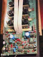


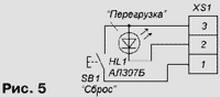


 ) and excess (current) noise, which manifests itself when current flows through the resistor and is caused by resistance fluctuations. In the audio frequency range, the magnitude of this noise for carbon resistors can exceed 10 μV (per decade of frequency at a voltage drop of 1 V). As a rule, this is an order of magnitude or more greater than the thermal noise of such a resistor.


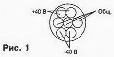

 Leave your comment on this article: