|
|


 Arabic
 Bengali
 Chinese
 English
 French
 German
 Hebrew
 Hindi
Hindi Italian
 Japanese
 Korean
 Malay
Malay Polish
 Portuguese
 Spanish
 Turkish
 Ukrainian
 Vietnamese
|
ENCYCLOPEDIA OF RADIO ELECTRONICS AND ELECTRICAL ENGINEERING Power amplifier with zero quiescent current output stage. Encyclopedia of radio electronics and electrical engineering
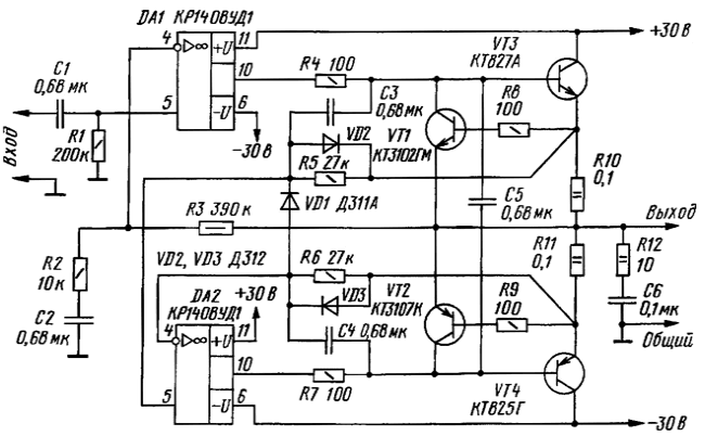
Encyclopedia of radio electronics and electrical engineering / Transistor power amplifiers From the prototype, which the readers of the magazine got acquainted with back in 1988, this amplifier differs in increased output power and protection of the output stage from short circuit. The amplifier draws very little current at rest, but when the signal is amplified, it goes into class AB mode with dynamic bias. The power amplifier, the circuit of which is shown in the figure, in many respects resembles the one published earlier by the author of this article in the journal [1], but the new one is much more powerful. Increasing the supply voltage was made possible through the use of high-voltage microcircuits. The device is supplemented with protection of powerful transistors against load short circuit. Main Specifications
A little about the operation of the amplifier. The input signal is fed to the non-inverting input of the op-amp DA1, it is amplified by about 40 times and from its output it is fed to the output transistor VT3, and through the capacitor C3 to the non-inverting input of the op-amp DA2. For the signal voltage based on the output stage transistor VT3, the op amp DA2 acts as a voltage follower (due to the presence of a feedback capacitor C4). At the same time, DA2 serves to monitor the quiescent current of the output stage by monitoring the voltage drop across resistors R10, R11. This voltage is amplified by the op amp and, together with the signal, is fed to the base of the transistor VT4 of the output stage, causing the pauses in the audio signal to reduce its current k to almost zero. This closing of the transistor VT4 could cause a change in the output voltage of the amplifier, however, the feedback voltage (in direct current) through the resistor R3, coming from the output of DA1 to the base of the transistor VT3, causes a corresponding decrease in its current, maintaining an average voltage at the output of the amplifier close to zero. When amplifying audio signals, capacitors C3-C5 are recharged by a pulsating voltage acting on the base-emitter junctions of powerful transistors. Therefore, the through current of the output stage at zero values of the signal voltage actually differs from zero and, depending on the level of audio signals, reaches 100 ... 150 mA. In the absence of a signal, diodes VD1-VD3 accelerate the process of switching to an economical rest mode, when powerful transistors are practically closed. Transistors VT1, VT2 protect the output stage from a short circuit of the load due to current feedback, using the voltage taken from the resistors R10, R11 in the emitter circuits of powerful transistors. As a result, the output current of the power stage is limited to about 6 A. The UMZCH can also be powered from a "unipolar" rectifier (without a midpoint). So, the output of an amplifier installed on a PBX and powered by a -60 V power supply is connected to the load through an oxide separating capacitor with a capacity of 2200 microfarads per 100 V. The power supply circuit VT3 and DA1 is connected to a common wire, and the voltage is connected to the lower output of the resistor R1, approximately equal to half the supply voltage, is supplied from a divider of two 100 kΩ resistors with a blocking oxide capacitor with a capacity of 200 microfarads per 50 V. With a load of 4 ohms, the output power of the UMZCH is slightly less than 100 W, so the dimensions of the heat sink must be at least 35x100x200 mm. The maximum current of the PSU rectifier (better than stabilized) must be at least 6 A. Mounting the amplifier is very simple, and the connections between the elements mounted on the board and the heatsink are made with a flexible wire. To connect the transistors of the output stage, it is recommended to use a wire with a cross section of at least 0,75 mm2. In the output stage, you can also use composite transistors of the complementary structure KT829A and KT853A or similar imported ones, or turn on separate high-frequency transistors of medium and high power, connecting them as composite transistors (according to the Darlington circuit). Instead of the transistors indicated on the diagram in positions VT1, VT2, you can install KT315B and KT361B, respectively. Capacitors C1 - C6 - K73-17. When using the K1408UD1 chip (foreign analogue - LM343) in the 301.8-1 package, one should keep in mind the differences in the pinout [2]. The amplifier practically does not need to be adjusted. When the amplifier is operating on a remote load connected via a long cable, it is recommended to connect the amplifier output to it through a parallel LR circuit made of a 2 Ohm MLT-10 resistor, on which the coil is wound with a PEV-2 wire with a diameter of 0,38 mm in one layer before filling. Literature
Author: L. Kompanenko, Moscow
Machine for thinning flowers in gardens
02.05.2024 Advanced Infrared Microscope
02.05.2024 Air trap for insects
01.05.2024
▪ Super high pressure in a new way ▪ High power controller with over 90% efficiency ▪ African fish can't stand the heat
▪ Modeling section of the site. Selection of articles ▪ article Roentgen Wilhelm. Biography of a scientist ▪ How Do Lemmings Die? Detailed answer ▪ ricin article. Legends, cultivation, methods of application
Home page | Library | Articles | Website map | Site Reviews
www.diagram.com.ua |

 Leave your comment on this article: