|
|


 Arabic
 Bengali
 Chinese
 English
 French
 German
 Hebrew
 Hindi
Hindi Italian
 Japanese
 Korean
 Malay
Malay Polish
 Portuguese
 Spanish
 Turkish
 Ukrainian
 Vietnamese
|
ENCYCLOPEDIA OF RADIO ELECTRONICS AND ELECTRICAL ENGINEERING Stereo amplifier with SPDIF input. Encyclopedia of radio electronics and electrical engineering
Encyclopedia of radio electronics and electrical engineering / Transistor power amplifiers The proposed powerful stereo UMZCH with SPDIF input is designed to amplify audio signals fed to its input from analog and digital sources. The rated output power of the amplifier is 2x25 W at a load of 4 ohms. Bandwidth - 0.02...20 kHz. The coefficient of non-linear distortion in the specified frequency band is not more than 0.15% (0,08% at a frequency of 1 kHz). The amplifier circuit is shown in fig. 1.
The SPDIF converter (LC + PC) is assembled on a DA1 chip (UDA1350ATS) manufactured by Philips. SPDIF (Sony/Philips Digital Interconnect Format) is a digital audio interface. In it, samples (signal samples) are transmitted at a fixed frequency, bit by bit, in blocks of 32 bits, where 8 bits (4 at the beginning and 4 at the end) are used for synchronization and service information, and 24 bits are used for information (Fig. 2 ).
In most cases, a 16-bit sample is transmitted (CDs contain only 16-bit "sound"), and the lower 8 bits are zero. This interface is very simple and cheap and therefore widely used. The SPDIF interface supports three standard sampling rates: 32; 44,1 and 48 kHz.
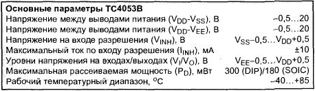
The UDA1350ATS, housed in a 28-pin SMD package, is a data stream recovery circuit for 24-bit stereo audio signal sampled at up to 48 kHz. The internal structure of the microcircuit is shown in fig. 3. When a signal appears at the SPDIF input, it is recognized by the decoder, processed, divided into two channels, the signals of which are converted to analog form and fed to the outputs (pins 15 and 17) DA1 (Fig. 1). The switching signal from pin 16 DA1 through a 2-transistor key VT1-VT2 acts on the switch DA2, which passes the decoded signals to the inputs of power amplifiers. Toshiba's TC4053B switcher is a 3-channel 2-way multiplexer that allows you to select analog and digital signals. The structure of the IC is shown in fig. 4. Depending on the logical levels at the address inputs A, B, C and the enable input 1NH, signals from one of the inputs (0X and 1X, 0Y or 1Y, 0Z or 1Z) pass to the outputs X, Y, Z. This commutation is reflected in the microcircuit's truth table.
At voltages VDD = + / -5 V. Vss = 0 V, VEE = -5 V, the signal can vary in the range -5 ... + 5 V. ICs are available in several types of packages: DIP16 (TC4053VR - Fig. 5a), SOP16 (TC4053BF - fig. 56), SOL16 (TC4053BFN - fig. 5c) and TSSOP16 (TC4053BFT - fig. 5d). The pinout of the microcircuit is shown in fig. 6. Power amplifiers DA3, DA4 (Fig. 1) are assembled on the LM2876 IC from National Semiconductor.
The LM2876 chip is an UMZCH with a maximum output power of 40 W at a load of 8 ohms and a harmonic coefficient of 0,1% in a frequency band of 0,02 .. .20 kHz. The IC has several protections (overload, overtemperature, power). It is produced in an 11-pin TO-220 package (Fig. 7).
The internal structure of the UMZCH is shown in fig. 8, and a typical switching circuit - in fig. 9.
The dependence of the harmonic coefficient K, on the frequency is shown in fig. 10, in fig. 11 - from the output power.
The dependence of the dissipated power on the output and output power on the supply voltage is shown by the graphs in fig. 12 and 13 respectively.
The SA2 button in the amplifier (Fig. 1) turns on the “Pause” (“Mute”) low power mode. The UMZCH is powered by a bipolar ± 25 V power supply. To power DA2, the positive supply voltage is reduced to 12 V by the DA6 integral stabilizer, and for DA1 - to 3.3 V, obtained using the DA5 stabilizer (AMS1117-3.3), manufactured by Advanced Monolithic Systems . When assembling the amplifier, the DA3, DA4 microcircuits are installed on a finned heat sink with an effective area of at least 100 cm2. Transformer T1 is wound on a toroidal core with a diameter of 100 mm and a cross section of 15x60 mm. The primary winding consists of 1250 turns of PEVTL-2 00,6 mm wire, and the secondary - 2x140 turns of PEVTL-2 01 mm. Establishing an amplifier correctly assembled from serviceable parts is not difficult. The signal from the sound generator with a frequency of 1 kHz is fed to the inputs of the LC and PC. A load is connected to the output of the amplifier, on which the output signal is monitored by an oscilloscope. Its shape should repeat the shape of the input signal. Author: V. Fedorov, G. Lipetsk
Artificial leather for touch emulation
15.04.2024 Petgugu Global cat litter
15.04.2024 The attractiveness of caring men
14.04.2024
▪ Stable miniature 3D airgel objects ▪ Transgenic product causes allergies ▪ Traces of early life in precious stones
▪ section of the site Electrical safety, fire safety. Article selection ▪ article Railroad tracks for the model. Tips for a modeler ▪ article Who recognized Hitler as the man of the year? Detailed answer ▪ article Weather Records. Sky. Travel Tips
Home page | Library | Articles | Website map | Site Reviews
www.diagram.com.ua |


 Leave your comment on this article: