|
|


 Arabic
 Bengali
 Chinese
 English
 French
 German
 Hebrew
 Hindi
Hindi Italian
 Japanese
 Korean
 Malay
Malay Polish
 Portuguese
 Spanish
 Turkish
 Ukrainian
 Vietnamese
|
ENCYCLOPEDIA OF RADIO ELECTRONICS AND ELECTRICAL ENGINEERING UMZCH with complementary field effect transistors. Encyclopedia of radio electronics and electrical engineering
Encyclopedia of radio electronics and electrical engineering / Transistor power amplifiers We present to readers a variant of a hundred-watt UMZCH with field-effect transistors. In this design, power transistor packages can be mounted on a common heat sink without insulating pads, and this significantly improves heat transfer. As the second version of the power supply, a powerful pulse converter is proposed, which should have a sufficiently low level of intrinsic noise. The use of field-effect transistors (FETs) in UMZCH until recently was constrained by a meager assortment of complementary transistors, as well as their low operating voltage. The quality of sound reproduction through the UMZCH on the FET is often rated at the level of the tube and even higher because, compared to amplifiers based on bipolar transistors, they create less non-linear and intermodulation distortion, and also have a smoother increase in distortion during overloads. They outperform tube amplifiers in both load damping and audio bandwidth. The cutoff frequency of such amplifiers without feedback is much higher than that of the UMZCH on bipolar transistors, which favorably affects all types of distortion. Nonlinear distortions in the UMZCH are mainly introduced by the output stage, and a common OOS is usually used to reduce them. Distortion in the input differential stage, used as an adder of signals from the source and the circuit of the common OOS, may be small, but with the help of the general OOS it is impossible to reduce them. The overload capacity of the differential stage on field-effect transistors is approximately 100 ... 200 times higher than with bipolar transistors. The use of field-effect transistors in the UMZCH output stage makes it possible to abandon the traditional two- and three-stage Darlington repeaters with their inherent disadvantages. Good results are obtained by using field-effect transistors with a metal-dielectric-semiconductor (MIS) structure in the output stage. Due to the fact that the current in the output circuit is controlled by the input voltage (similar to electrovacuum devices), then at high currents the speed of the cascade on MIS field-effect transistors in the switching mode is quite high (τ = 50 ns). Such cascades have good transmission properties at high frequencies and have the effect of temperature self-stabilization. The advantages of field effect transistors include:
But besides the advantages, these devices also have disadvantages:
The last of the noted shortcomings limits the output power, especially at low supply voltages; the way out is the parallel connection of transistors and the introduction of environmental protection. It should be noted that recently foreign firms (for example, Exicon, etc.) have developed a lot of field-effect transistors suitable for audio equipment: EC-10N20, 2SK133-2SK135, 2SK175, 2SK176 with an n-type channel; EC-10P20, 2SJ48- 2SJ50, 2SJ55, 2SJ56 with p-channel. Such transistors are characterized by a weak dependence of the slope (forward transfer admitance) on the drain current and smoothed output I–V characteristics. The parameters of some field-effect transistors, including those manufactured by the Minsk Production Association "Integral", are given in Table. 1.
Most transistor transformerless UMZCH are made according to a half-bridge circuit. In this case, the load is included in the diagonal of the bridge formed by two power supplies and two output transistors of the amplifier (Fig. 1).
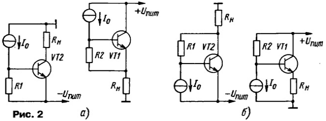
When there were no complementary transistors, the UMZCH output stage was performed mainly on transistors of the same structure with a load and a power source connected to a common wire (Fig. 1, a). Two possible options for controlling the output transistors are shown in fig. 2.
In the first of them (Fig. 2, a), the control of the lower arm of the output stage is in more favorable conditions. Since the change in the supply voltage is small, the Miller effect (dynamic input capacitance) and the Earley effect (collector current versus emitter-collector voltage) practically do not appear. The control circuit of the upper arm is connected here in series with the load itself, therefore, without taking additional measures (for example, cascode switching of devices), these effects are manifested to a large extent. According to this principle, a number of successful UMZCHs have been developed [1-3]. According to the second option (Fig. 2,6 - MIS transistors are more suitable for such a structure), a number of UMZCHs were also developed, for example [4, 5]. However, even in such cascades it is difficult to ensure, even with the use of current generators [5], the control symmetry of the output transistors. Another example of input impedance balancing is the implementation of the amplifier arms according to a quasi-complementary scheme or the use of complementary transistors (see Fig. 1,b) in [6]. The desire to balance the arms of the output stage of amplifiers made on transistors of the same conductivity led to the development of amplifiers with an ungrounded load according to the circuit in Fig. 1,d [7-9]. However, even here it is not possible to achieve complete symmetry of the previous cascades. The negative feedback circuits from each arm of the output stage are unequal; NFB circuits of these cascades [7, 8] control the voltage at the load in relation to the output voltage of the opposite arm. In addition, such a circuit solution requires isolated power supplies. Due to these shortcomings, it has not found wide application. With the advent of complementary bipolar and field-effect transistors, the output stages of the UMZCH are mainly built according to the circuits in Fig. 1b, c. However, even in these variants, high-voltage devices must be used to drive the output stage. The transistors of the pre-output stage operate with a high voltage gain, and therefore are subject to the Miller and Earley effects and, without a common OOS, introduce significant distortion, which requires high dynamic characteristics from them. Feeding the preliminary stages with increased voltage also reduces the efficiency of the amplifier. If in Fig. 1, b, c move the connection point with the common wire to the opposite shoulder of the diagonal of the bridge, we get the options in fig. 1,e [10] and 1,f, respectively. In the structure of the cascade according to the scheme of Fig. 1e automatically solves the problem of isolating the output transistors from the case. Amplifiers made according to such schemes are free from a number of the listed disadvantages. Amplifier circuitry features The attention of radio amateurs is offered an inverting UMZCH (Fig. 3), corresponding to the block diagram of the output stage in Fig. 1, e.
The input differential stage is made on field-effect transistors (VT1, VT2 and DA1) according to a symmetrical circuit. Their advantages in the differential stage are well known: high linearity and overload capacity, low noise. The use of field-effect transistors greatly simplified this cascade, since there was no need for current generators. To increase the gain with an open loop OS, the signal is taken from both shoulders of the differential stage, and an emitter follower on transistors VT3, VT4 is installed in front of the subsequent voltage amplifier. The second stage is made on transistors VT5-VT10 according to a combined cascode circuit with servo power. Such a power supply of the cascade with OE neutralizes the input dynamic capacitance in the transistor and the dependence of the collector current on the emitter-collector voltage. The output stage of this stage uses high-frequency BSIT transistors, which, compared to bipolar ones (KP959 versus KT940), have twice the cutoff frequency and four times the drain (collector) capacitance. The use of an output stage powered by separate isolated sources made it possible to dispense with a low-voltage supply (9 V) for the preamplifier. The output stage is made on powerful MIS transistors, and the conclusions of their drain (and heat-removing flanges of the housings) are connected to a common wire, which simplifies the design and assembly of the amplifier. Powerful MIS transistors, unlike bipolar ones, have a smaller spread of parameters, which facilitates their parallel connection. The main spread of currents between devices arises due to the inequality of threshold voltages and the spread of input capacitances. The introduction of additional 50-200 Ohm resistors in the gate circuits provides almost complete equalization of the turn-on and turn-off delays and eliminates current spread during switching. All stages of the amplifier are covered by local and general environmental protection. Main Specifications
With OS enabled
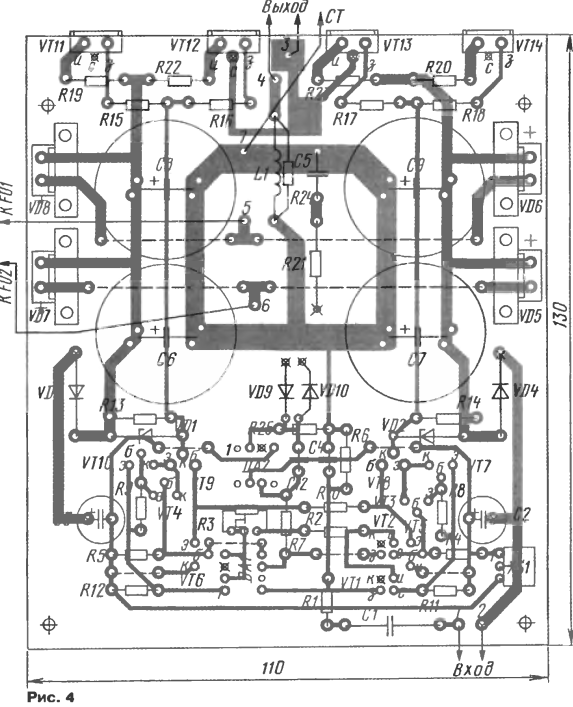
Due to the relatively high cutoff frequency of an open-loop feedback amplifier, the feedback depth and harmonic distortion are nearly constant across the entire frequency range. From below, the operating frequency band of the UMZCH is limited by the capacitance of capacitor C1, from above - by C4 (with a capacitance of 1,5 pF, the cutoff frequency is 450 kHz). Construction and details The amplifier is made on a board made of double-sided foil fiberglass (Fig. 4).
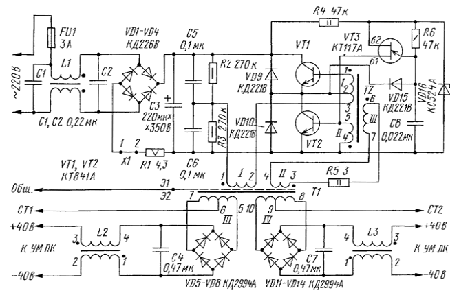
The board from the side where the elements are installed is maximally filled with foil connected to a common wire. Transistors VT8, VT9 are equipped with small plate heat sinks in the form of a "flag". Pistons are installed in the holes for the drain terminals of powerful field-effect transistors; the drain terminals of transistors VT11, VT14 are connected to a common wire from the side of the foil (marked with crosses in the figure). Pistons are installed in holes 5-7 of the board for connecting the mains transformer leads and jumper holes. Resistors R19, R20, R22, R23 are made of manganin wire with a diameter of 0,5 and a length of 150 mm. To suppress the inductance, the wire is folded in half and folded (bifilar) is wound on a mandrel with a diameter of 4 mm. The inductor L1 is wound with a PEV-2 wire 0,8 turn to turn over the entire surface of a 2 W resistor (MLT or similar). Capacitors C1, C5, C10, C11 - K73-17, and C10 and C11 are soldered from the PCB side to the terminals of capacitors C8 and C9. Capacitors C2, C3 - oxide K50-35; capacitor C4 - K10-62 or KD-2; C12 - K10-17 or K73-17. Field-effect transistors with an n-channel (VT1, VT2) must be selected with approximately the same initial drain current as the transistors in the DA1 assembly. In terms of cutoff voltage, they should not differ by more than 20%. Microassembly DA1 K504NTZB can be replaced by K504NT4B. It is possible to use a matched pair of transistors KP10ZL (also with indices G, M, D); KP307V - KP307B (also A, E), KP302A or transistor assembly KPC315A, KPC315B (in this case, the board will have to be reworked). In positions VT8, VT9, you can also use complementary transistors of the KT851, KT850 series, as well as KT814G, KT815G (with a cut-off frequency of 40 MHz) of the Minsk Association "Integral". In addition to those indicated in the table, you can use, for example, the following pairs of MIS transistors: IRF530 and IRF9530; 2SK216 and 2SJ79; 2SK133-2SK135 and 2SJ48-2SJ50; 2SK175-2SK176 and 2SJ55-2SJ56. For the stereo version, power is supplied to each of the amplifiers from a separate transformer, preferably with a ring or rod (PL) magnetic circuit, with a power of 180 ... 200 W. Between the primary and secondary windings, a layer of shielding winding is placed with a wire PEV-2 0,5; one of its conclusions is connected to a common wire. The outputs of the secondary windings are connected to the amplifier board with a shielded wire, and the shield is connected to the common wire of the board. Windings for the rectifiers of the preamplifiers are placed on one of the network transformers. Voltage stabilizers are made on IL7809AC (+9 V), IL7909AC (-9 V) microcircuits - not shown in the diagram. The ONp-KG-2-9 (XS26) connector was used to supply the 3x1 V power board. When setting up, the optimal current of the differential stage is set by a tuned resistor R3 to minimize distortion at maximum power (approximately in the middle of the working area). Resistors R4, R5 are designed for a current of about 2...3 mA in each arm with an initial drain current of about 4...6 mA. With a lower initial drain current, the resistance of these resistors must be proportionally increased. The quiescent current of the output transistors in the range of 120 ... 150 mA is set by a trimming resistor R3, and, if necessary, by selecting resistors R13, R14. Impulse power block For those radio amateurs who have difficulty purchasing and winding large network transformers, a switching power supply is offered for the UMZCH output stages. In this case, the preamplifier can be powered from a low-power stabilized PSU. A pulsed power supply unit (its circuit is shown in Fig. 5) is an unregulated self-generating half-bridge inverter. The use of proportional-current control of the inverter transistors in combination with a saturable switching transformer makes it possible to automatically remove the active transistor from saturation by the time of switching. This reduces the charge dissipation time in the base and eliminates the through current, and also reduces power losses in the control circuits, increasing the reliability and efficiency of the inverter.
UPS specifications
An interference suppression filter L1C1C2 is installed at the input of the mains rectifier. Resistor R1 limits the inrush charging current of capacitor C3. A jumper X1 is provided in series with the resistor on the board, instead of which you can turn on a choke to improve filtering and increase the "hardness" of the output load characteristic. The inverter has two positive feedback circuits: the first - by voltage (using windings II in transformer T1 and III - in T2); the second - by current (with a current transformer: turn 2-3 and windings 1-2, 4-5 of transformer T2). The trigger device is made on a unijunction transistor VT3. After starting the converter, it turns off due to the presence of the VD15 diode, since the time constant of the R6C8 circuit is much larger than the conversion period. The peculiarity of the inverter is that when low-voltage rectifiers operate on large filter capacities, it needs a smooth start. The smooth start of the block is facilitated by the chokes L2 and L3 and, to some extent, the resistor R1. The power supply is made on a printed circuit board made of one-sided foil fiberglass 2 mm thick. The board drawing is shown in fig. 6.
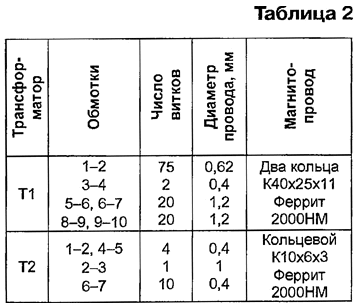
The winding data of transformers and information about the magnetic circuits are given in Table. 2. All windings are made with PEV-2 wire.
Before winding the transformers, the sharp edges of the rings must be blunted with sandpaper or a bar and wrapped with varnished cloth (for T1 - rings folded together in three layers). If this pre-treatment is not done, then it is possible that the varnished fabric will be pressed through and the turns of the wire will be shorted to the magnetic circuit. As a result, the no-load current will increase sharply and the transformer will heat up. Between the windings 1-2, 5-6-7 and 8-9-10, shielding windings are wound with PEV-2 0,31 wire in one layer turn to turn, one end of which (E1, E2) is connected to a common UMZCH wire. The winding 2-3 of the transformer T2 is a coil of wire with a diameter of 1 mm over the winding 6-7, soldered by the ends into the printed circuit board. Inductors L2 and L3 are made on BZO armored magnetic cores made of 2000NM ferrite. The windings of the chokes are wound in two wires until the frame is filled with PEV-2 0,8 wire. Given that the chokes operate with DC bias, it is necessary to insert spacers of non-magnetic material 0,3 mm thick between the cups. The L1 choke is of the D13-20 type, it can also be made on the B30 armored magnetic circuit similarly to the L2, L3 chokes, but without a gasket, by winding the windings in two MGTF-0,14 wires until the frame is filled. Transistors VT1 and VT2 are mounted on heat sinks made of ribbed aluminum profile with dimensions of 55x50x15 mm through insulating gaskets. Instead of those indicated in the diagram, you can use the KT8126A transistors of the Minsk software "Integral", as well as MJE13007. Additional oxide capacitors K40-40 (not shown in the diagram) with a capacity of 1 μF per 2 V are connected between the PSU outputs +50 V, -6 V and "its" midpoint (ST2000 and ST50). These four capacitors are installed on a textolite plate with dimensions 140x100 mm, fixed with screws on the heat sinks of powerful transistors. Capacitors C1, C2 - K73-17 for a voltage of 630 V, C3 - oxide K50-35B for 350 V, C4, C7 - K73-17 for 250 V, C5, C6 - K73-17 for 400 V, C8 - K10-17 . The pulse PSU is connected to the PA board in close proximity to the terminals of the capacitors C6-C11. In this case, the VD5-VD8 diode bridge is not mounted on the PA board. To delay the connection of acoustic systems to the UMZCH for the time of attenuation of transients that occur during power-up, and turn off the speakers when a constant voltage of any polarity appears at the output of the amplifier, you can use the simplest [10] or more complex protective device. Literature
Author: A.Petrov, Mogilev, Belarus
The world's tallest astronomical observatory opened
04.05.2024 Controlling objects using air currents
04.05.2024 Purebred dogs get sick no more often than purebred dogs
03.05.2024
▪ Bacteria that feed on air discovered ▪ Signal circuit boards found inside human cells ▪ Impossible black hole discovered
▪ section of the site Standard instructions for labor protection (TOI). Selection of articles ▪ article Forbidden fruit is sweet. Popular expression ▪ article What are mushrooms? Detailed answer ▪ article Manufacturer of casein. Job description
Home page | Library | Articles | Website map | Site Reviews
www.diagram.com.ua |


 Leave your comment on this article: