|
|


 Arabic
 Bengali
 Chinese
 English
 French
 German
 Hebrew
 Hindi
Hindi Italian
 Japanese
 Korean
 Malay
Malay Polish
 Portuguese
 Spanish
 Turkish
 Ukrainian
 Vietnamese
|
ENCYCLOPEDIA OF RADIO ELECTRONICS AND ELECTRICAL ENGINEERING Transceiver Amator-EMF-M. Encyclopedia of radio electronics and electrical engineering
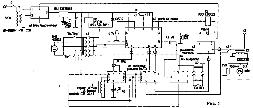
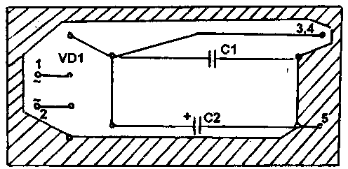
Encyclopedia of radio electronics and electrical engineering / Civil radio communications The transceiver is designed for radio communication in SSB and CW modes in the amateur radio bands of 160, 80 and 40 meters. The low-signal part of the "Amator-EMF" transceiver [1] was taken as a basis. The sensitivity of the transceiver with a signal-to-noise ratio of 10 dB is no worse than 1 μV. Mirror channel selectivity - not less than 40 dB, RDD range - more than 60 dB, output power at a load of 50 Ohms - not less than 8 W, side channel suppression - not worse than 40 dB. The selectivity of the transceiver for the adjacent channel during reception and the suppression of the non-working sideband during transmission are determined by the characteristics of the electromechanical filter. The block diagram of the transceiver is shown in Fig. 1. When receiving a signal from the antenna through connector X3 and contacts K2.1, relay K2 enters the board of dual-circuit filters A5.
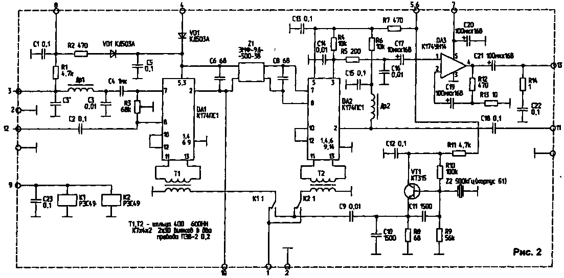
The signal is then sent to the main board A2. The signal of the smooth range generator from the A4 board is also supplied here. The processed and amplified signal is output to the dynamic head WA. When transmitting, the signal from the electret microphone BM1 is fed to pin 3 of the A2 board. From output 11 of the A2 board, the generated SSB signal is fed to the A5 bandpass filter board. From pin 4 of board A5, the signal is fed to power amplifier A3. From the A3 board, the amplified signal through the contacts of the relay K2.1 goes to the X3 connector and from there goes to the antenna. The T2 current sensor is wound on a 600NN ring, put on the antenna wire, and contains 6 turns of PELSHO-0,2 wire. When CW is running, pin 10 of board A2 receives a 501 kHz signal from board A6 of the telegraph local oscillator. The diagram of the main board A2 is shown in Fig.2. The main elements of the transceiver path A2 are active balanced mixers K174PS1. This made it possible to simplify the electrical circuit. DA3 (K174UN14) - low frequency amplifier. A reference frequency generator is assembled on VT1. The main selection during reception and the formation of the SSB signal during transmission are performed by an electromechanical filter EMF-9D-500-ZV. Relays K1 and K2 switch the signals of the smooth range generator and the reference frequency generator during the transition from reception to transmission.
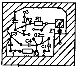
Figure 3 shows a diagram of a smooth range generator. A distinctive feature of this circuit is the use of an analog of a lambda diode as a generating element (VT2, VT3). This circuit operates at low voltages (2,5 V) and low currents (200 ... 250 μA). This eliminates the heating of the frequency-setting elements, which, in turn, leads to a minimum initial frequency overrun and high stability.
The analogue of the lambda diode is powered by a voltage regulator on DA1 with a high stabilization factor. This made it possible to obtain a frequency drift of less than 60 Hz when the supply voltage changed from 10 to 15 V. A frequency doubler was assembled on VD1, VD2 and T1. GPA frequencies are shown in the table.
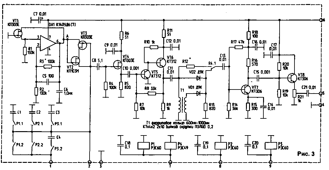
By selecting a resistor R3 at point A, a voltage of 2,5 ... 2,65 V is set. Capacitors C1 ... C4 lay the GPA tuning range. C4 stretches the 7 MHz range to full scale. With the help of R12, the amplitude of the RF voltage is equalized in the modes with and without doubling the frequency. Power amplifier A3 (Fig. 4) - three-stage. The amplifier does not have switching elements when switching from range to range, and frequency overlap from 1,8 to 7 MHz is provided by changing the capacitance of the variable capacitor C1.
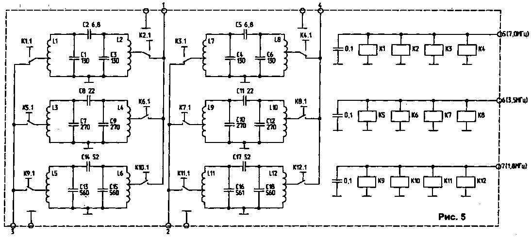
T1 - ferrite ring 600NN...1000NN K10x6x4, 2x10 turns of PELSHO-0,31 twist. L1 - ferrite ring 50 HF K32x16x8, 14 turns PEL-0,8, taps - from the 2nd and 4th turns. The ring should be wrapped with fluoroplastic tape so as not to damage the wire insulation. The A5 bandpass filter board (Fig. 5) has no special features. L1, L3 - 27 + 9 turns of PELSHO-0,2 wire; L2, L7 - 18 + 8 turns of PELSHO-0,2 wire; L3, L10 - 40 + 10 turns of PELSHO-0,1 wire; L4, L9 - 25+25 turns of PELSHO-0,1 wire; L5, L12 turns of wire PELSHO-0,1; L6, L11 - 35+35 turns of PELSHO-0,1 wire. Frameworks - with a diameter of 5 mm with trimming cores from SB-12A.
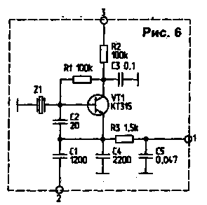
Relay K1...K12 - RES-49. Instead of a relay, you can use a button switch. A feature of the A6 board of the CW generator (Fig. 6) is the use of a piezoceramic disk taken from the PF1P filter from old transistor portable radio receivers as a frequency-setting element.
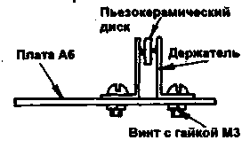
The filter cover is carefully separated with a knife or a hacksaw. The filter is a plastic base with eight cells, closed with two getinax sidewalls. Between the sidewalls, in the cells, piezoceramic discs are fixed with the help of silver-plated spring washers. Carefully drilling out two aluminum rivets, we disassemble the filter. The filter contains four thin discs and four thick ones. Thick discs are suitable for making a resonator. We make a CW generator board and a disk mount. The disc mount can be made from two strips of phosphor bronze or other springy material (Figure 7).
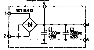
Stepping back 3 mm from the end of the strip, we make notches with a center punch. It is important that when installing the holders on the board, the notches are located exactly one opposite the other so that there is no skew when installing the disk. We close output 1 of the A6 board to a common wire, connect a frequency meter to output 2, and supply power to output 3. We insert a disk between the holders and measure the frequency. The frequency is adjusted by reducing the diameter of the disc by turning it around the circumference on an emery cloth - "zero" or using a diamond file. The disk is turned until the generation frequency of 500.7 ... 501 kHz is obtained. It is necessary to control the frequency during the fitting process as often as possible. The stability of such an oscillator is sufficient to be used as a 500 kHz reference oscillator. The diagram of the block of rectifiers A1 is shown in Fig. 8.
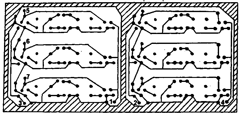
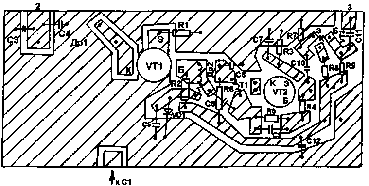
Figures 9...14 show drawings of printed circuit boards on a scale of 1:1 with the arrangement of elements. In the power amplifier board (Fig. 14), holes with a diameter of 1 mm are made under VT2 and VT12. Transistors VT1 and VT2 are mounted on a radiator. The radiator is made of a duralumin plate 130x60 mm in size and 4...5 mm thick. The printed circuit board is fixed above the heatsink with 3 mm high posts. Installation is carried out by a hinged method from the side of the printed conductors.
The location of the boards in the transceiver is arbitrary. The only desirable condition is shielding from the A2 and A5 boards of the power amplifier board. The establishment of the transceiver begins with the A4 board. The adjustment comes down to laying the ranges using C1 ... C4 and adjusting the output voltage using R21 within 400 ... 500 mV. Resistor R3 is temporarily replaced by a variable one, and with its help, at point A, the voltage is set within 2,5 ... 2,6 V. Then, having measured the resulting resistance, they select the closest one at face value and put it in place of R3. Having connected the GPA and band-pass filters to the main board A2, the A2 and A5 boards are configured. Having tuned in to any station, with the help of cores, the output band-pass filters are adjusted to the maximum reception volume. By selecting C6 and C8, the input and output coils of the EMF are tuned. Resistor R12 select the required gain ULF DA3. After that, they proceed to setting up the transmitting path. The transceiver is put into transmit mode. By applying a signal with a level of 3 ... 5 mV from the audio signal generator to the microphone input, the band-pass filters of the transmitting path are adjusted to the maximum output voltage. After that, turning off the sound generator or turning off the telegraph generator, they close the conclusions 2 ... 3 of the main board with a jumper. By connecting a voltmeter or an oscilloscope to the output of the band-pass filters of the transmitting path, the carrier level is monitored. Using R3 of the A2 board, they achieve maximum carrier suppression (minimum output voltage). Having connected all the boards according to Fig. 1, they carry out the final adjustment of all the boards with the corresponding adjusting elements. By connecting a load resistor with a resistance of 3 ohms and a power of at least 50 W to the antenna jack X12 (6 pieces of MLT-2 resistors with a resistance of 300 ohms connected in parallel), the output voltage is controlled, which should be within 20 ... 25 V. Literature
Author: I.Ptashnik (UY5UM), Kiev region, Buga settlement; Publication: N. Bolshakov, rf.atnn.ru
The world's tallest astronomical observatory opened
04.05.2024 Controlling objects using air currents
04.05.2024 Purebred dogs get sick no more often than purebred dogs
03.05.2024
▪ New two-stage current sensors ▪ Google Edge TPU microprocessor for machine learning algorithms ▪ Coronavirus vaccine in the form of a patch
▪ section of the site Encyclopedia of radio electronics and electrical engineering. Article selection ▪ article Leibniz Gottfried. Biography of a scientist ▪ article Which plant flowers become transparent after rain? Detailed answer ▪ article Predicting the weather at sea. Travel Tips ▪ article Universal metal detector. Encyclopedia of radio electronics and electrical engineering ▪ article Dual-band antenna amplifier. Encyclopedia of radio electronics and electrical engineering
Comments on the article: Torbik Sergey Vitalievich Please explain how many turns does the L5 and L12 coil have in the bandpass filter board?
Home page | Library | Articles | Website map | Site Reviews
www.diagram.com.ua |


 Leave your comment on this article: