|
|


 Arabic
 Bengali
 Chinese
 English
 French
 German
 Hebrew
 Hindi
Hindi Italian
 Japanese
 Korean
 Malay
Malay Polish
 Portuguese
 Spanish
 Turkish
 Ukrainian
 Vietnamese
|
ENCYCLOPEDIA OF RADIO ELECTRONICS AND ELECTRICAL ENGINEERING Scheme for protecting the on-board network from the surge of charge current when an uncharged capacitor is turned on
Encyclopedia of radio electronics and electrical engineering / Automobile. Electronic devices The circuit is designed to protect against the surge of the charge current when an uncharged capacitor is connected to the on-board network. Whoever has not tried to include an uncharged faradnik in the network without a limiting resistor - better not ... At a minimum, the contacts will burn.
When the discharged capacitance is connected to the network, the capacitance C1 is discharged, T1 (n-MOS switch with low channel resistance) is closed. Capacitance C2 (the same faradnik) is charged through low-resistance R5. T2 opens almost instantly, I shunt C1 to ground and T1 gate. When the potential of the negative terminal C2 drops below 1V (charging to Vacb - 1V), T2 closes, C1 smoothly charges to about 9/10 Vacb, opening T1. The time constant R2C1 is large enough so that the current surge T1 (recharging C2 by + 1V to Uakb) does not exceed the allowable for T1. In the future, the negative terminal C2 is constantly closed to ground through T1, REGARDLESS OF THE DIRECTION OF THE CURRENT T1 (both in the forward direction - from the drain to the source, and in the opposite direction). There is nothing wrong with "turning over" an OPEN MIS transistor. When choosing a fairly well-conducting transistor, the entire reverse current will flow through the channel, and the built-in reverse diode will not open, since the voltage drop across the channel is several times less than the 0.5-0.8 V required for opening. By the way, there is a whole class of MIS devices (the so-called FETKY ), designed specifically to work in the opposite direction (synchronous rectifiers), they have a built-in diode shunted by an additional power Schottky diode. Calculation: for the IRF1010 transistor (Rds=0.012 ohm), the voltage drop of 0.5 ohm will be achieved only at a channel current of 40A (P=20W). For four such transistors in parallel and the same discharge current of 40A, each transistor will dissipate 0.012 * (40/4) ^ 2 = 1.2 W, i.e. They won't need heatsinks (especially since 1.2W will be dissipated only when the current consumption fluctuates, but not constantly). With tight mounting (do you have a lot of space for an extra radiator?) - it is advisable to parallel small-sized (TO251, DIP4 package) transistors that do not provide for radiators at all, based on the ratio of current (power) consumption of the amplifier - Rds - maximum dissipated power. Since Pds max is typically 1W (800mW for DIP4), the amount n transistors (with Rds each) for an amplifier with output power Pout must be at least n > 1/6 * Pout * sqrt(Rds) at 12V supply (I omitted the dimensions in the formula). In fact, taking into account the short duration of current pulses, n can be safely halved compared to this formula. The charge resistor R5 is selected from a compromise of thermal power and charge time. With the specified 22 ohms, the charge time is about 1 minute with a power dissipation of 7 watts. You can turn on a 5V bulb instead of R12, say, from a turn signal. Resistors R1, R3 - reinsurance (discharge capacity when disconnected from the network). To indicate the inclusion, we connect an additional inverter (reducing R2). Attention! The circuit is operational when using npn transistors T2, T3 with h21e\u200e 3102 (KT1). Depending on the brightness of the LED, select R200 in the range of 1 Ohm - XNUMXkOhm.
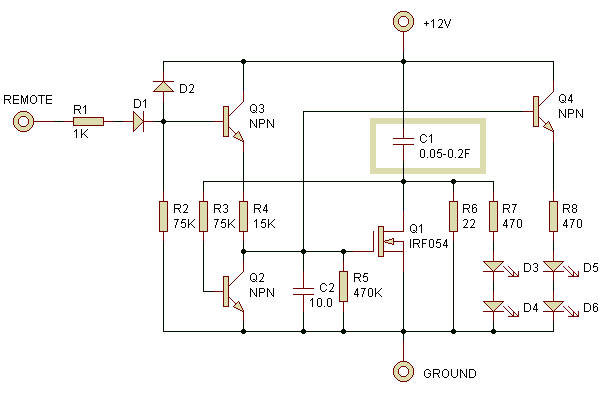
And here is a variant of the circuit in which the gate switch is controlled by the REMOTE signal (transistor AND). When REMOTE is not connected or turned off, the key transistor is guaranteed to be closed. LEDs D3-D4 indicate charging C1, D5-D6 - the open state of the key.
Accurate indication of the mains voltage threshold is most easily provided by the TL431 (KR142EN19) IC in the typical voltage comparator mode (with an appropriate divider in the input circuit and current-limiting R in the cathode circuit). The losses of the circuit are largely dependent on the installation. It is necessary to provide a minimum resistance (and current-appropriate wire thicknesses) in the power circuit (terminal + / C2 / T1 / terminal -). In amateur practice, I think it is impractical to make external terminals - it is better to immediately unsolder the short AWG8 wires with which the circuit is tied to the amplifier terminal block. Publication: klausmobile.narod.ru
Machine for thinning flowers in gardens
02.05.2024 Advanced Infrared Microscope
02.05.2024 Air trap for insects
01.05.2024
▪ Cutlery affects the taste of food ▪ D-Link DCS-8325LH Cloud Wireless Camera ▪ Adults evaluate children according to words ▪ Transformer on vegetable oil
▪ site section Clocks, timers, relays, load switches. Article selection ▪ article by Mikhail Ostrogradsky. Biography of a scientist ▪ article Insole with electric heating. Encyclopedia of radio electronics and electrical engineering
Home page | Library | Articles | Website map | Site Reviews
www.diagram.com.ua |


 Leave your comment on this article: