|
|


 Arabic
 Bengali
 Chinese
 English
 French
 German
 Hebrew
 Hindi
Hindi Italian
 Japanese
 Korean
 Malay
Malay Polish
 Portuguese
 Spanish
 Turkish
 Ukrainian
 Vietnamese
|
ENCYCLOPEDIA OF RADIO ELECTRONICS AND ELECTRICAL ENGINEERING CONTEST transceiver. Encyclopedia of radio electronics and electrical engineering
Encyclopedia of radio electronics and electrical engineering / Civil radio communications The name of Vladimir Rubtsov (UN7BV) - an engineer, artist, former pilot, crew commander - is well known to readers of KV Zhurnal, where he began publishing in 1993. Vladimir devotes all his free time to designing amateur communications equipment and working on the air. He is the author of more than a dozen journal publications, the book "Amateur Radio Transceiver Equipment UN7BV". Today we present one of his latest developments - the "CONTEST" transceiver. Radio amateurs involved in the design of amateur transceivers, when choosing a device construction scheme, in particular its intermediate frequency, along with the traditional factors that determine this choice, also have appeared not quite ordinary ones. These include the cost of radio components, the prevalence of certain of them in the CIS countries and the ability to purchase them, or, in general, the opportunity (considering the price) to buy a good imported device and, thus, solve the indicated problem. In the transceiver "CONTEST" offered to the attention of readers, an IF of 10,7 MHz is used. Its use in a device designed to operate on all amateur bands, including WARC, is not optimal (compared, for example, with a 5,5 MHz IF) due to the presence of affected points in the 14 and 21 MHz bands and the complexity of constructing the VFO. However, the prevalence of quartz filters at a frequency of 10,7 MHz in the CIS countries, their low price were a serious argument in favor of the choice made. The above "minuses" when using such an IF were eliminated in the transceiver by using appropriate circuit solutions, namely: choosing the GPA frequency above the IF in the above ranges, followed by a sideband "flip" in the IF path. The main technical characteristics of the transceiver:
The block diagram of the transceiver, combined with the connection diagram of the nodes, is shown in fig. 1, schematic diagrams of nodes - in fig. 2-17. The device is a superheterodyne with one fixed intermediate frequency and reverse amplification paths. Operating voltages +12 V (RX) and +12 V (TX) are taken from the cathodes of the VD68 and VD69 diodes (Fig. 1), respectively. Relays K11, K12, K16 and K17 are used to switch the transceiver from receive mode to transmit mode and vice versa. The HL2 incandescent lamp with a blue color filter is designed to indicate the transceiver is on and to illuminate the Smeter PA1 scale, the HL1 lamp with a red color filter indicates that the device is in transmission mode.
Relays K13, K14 and switch SB2 ("UP") provide switching of the quartz filter to narrow band mode, pushbutton switch SB4 ("CW") switches the transceiver to telegraph mode, and SB5 ("VOX") - to telephone voice control mode. The SB6 ("RX") button is used in receive mode. If it is not pressed (that is, it is in the position shown in Fig. 1), then it is possible to transmit SSB using the SA6 push-to-talk (it is used to put the transceiver into transmission mode in all modes if SB6 is not pressed). If the button is pressed, then the transceiver is also in the receive mode, it is impossible to transmit using the PTT in SSB mode, however, you can work with the telegraph through the VOX system using the tone generator of the electronic telegraph key. Button SB7 "Adjust." ("Setup") the transceiver is put into setup mode. At the same time, it switches to the TX mode (without pressing the PTT), at the same time the telegraph local oscillator is turned on in the constant radiation mode. A tone with a frequency of about 1 kHz is heard from the speaker driver BA1. The SB8 button is used to transfer the transceiver to the transmission mode without using the PTT, while it is possible to work both by CW and SSB. The detuning mode is turned on with the SB1 button, the frequency is changed with a variable resistor R203. Relay contacts K17.1 are used to control an additional power amplifier, K17.2 - to generate operating voltages of +12 V (RX) and +12 V (TX), relay contacts K15.2 and K15.3 - to control the reverse IF. Switch SB9 serves to disable the AGC system. The variable resistor R204 regulates the level of self-listening of the tone generator in CW mode, the resistor R201 - gain for transmission.
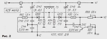
In the receive mode, the RF signal from the XW1 antenna socket (Fig. 1) through the SWR meter (Fig. 2, terminals 40, 41) enters the P-loop L16 (Fig. 3, terminal 52), then through terminal 6, relay contacts K11.1. 55, capacitor C1.3 and section SA4 of the range switch (Fig. 8) - to the L63C7 circuit and then amplified by a bidirectional (reversing) cascade on transistors VT8, VTXNUMX.
In the considered mode, the RF signal passes in the direction from L8 to C67 through the transistor VT8, in the transmission mode - from C67 to L8 through the transistor VT7. The transfer of the cascade from the RX mode to the TX mode is carried out by applying a voltage of +12 V to pins 10 (RX) and 9 (TX). In this case, the transistor VT8 is connected according to the circuit with a common source, and VT7 - with a common base. As a result, the input / output resistances of the stages in both modes are high on the side of the L8C63 circuit and low on the side of the capacitor C67 and the diode balanced mixer following it, which favorably affects the matching of the input / output resistances of adjacent stages.
The connection of the emitter of the transistor VT7 through the inductor L9 and the resistor R33 with the source VT8 contributes to the closing of the non-working transistor VT7 in the RX mode due to the supply of a small positive voltage to it from the source of the VT8 operating in this mode. In transmit mode, the closing process is reversed. The AGC voltage is applied to the second gate VT8 in the RX mode, and in the TX mode - a closing voltage of negative polarity. From the drain of the transistor VT8, the amplified RF signal through the capacitor C67 is fed to a double bridge balanced mixer (Fig. 5). It consists of two diode bridges (VD18-VD21 and VD22-VD25), transformers T3, T4 and resistors R40, R41. The presence of the latter makes it possible to implement the switching mode of diodes at a relatively high local oscillator voltage (effective value 4 V) and to limit the current through the diodes during the opening half-wave of voltage to the maximum permissible values.
The described node is one of the options for a high-level mixer capable of providing a large dynamic range due to the high local oscillator voltage, as well as a high level of input signal suppression. The positive qualities of such a mixer also include a good decoupling of the input and heterodyne circuits and its reversibility, i.e., the ability to work in different signal path directions. The GPA signal is fed to one of the windings of the transformer T3 (pin 20), and the RF signal is fed through pin 26 and capacitor C100 to the connection point of the two windings of the transformer T4. The 10,7 MHz IF signal in receive mode is taken from its third winding, which, together with capacitor C102, forms an IF preselection filter. From this filter, through the capacitor C101, the IF signal is fed to the input of a bidirectional amplifier made on transistors VT9-VT11. In the receive mode (passage of the signal from the capacitor C101 to C103), the cascode amplifier operates on transistors VT9 and VT10 (the first is connected according to the common source circuit, the second - according to the common base circuit), in the transmission mode (signal flow from C103 to C101) - one transistor VT11. Such a circuit design allows you to obtain the necessary amplification of the IF signal in both modes (RX and TX). In the first case, a control voltage is supplied to the second gate of the VT9 transistor either from the AGC system or from the resistor R131 (through the cascade on the VT26 transistor) in order to adjust the IF gain. In TX mode, this gate VT9 receives a closing voltage of negative polarity through resistor R202, generated by a generator based on transistors VT41, VT42, located on a digital scale. The same closing voltage is applied to the second VT11 gate in RX mode. In transmit mode, it receives a gain control voltage (DSB) from resistor R201 (see Fig. 1). The IF signal, selected by the filter L11C106 (Fig. 5), through the coupling coil L12 and the capacitor C103 (from pin 21) enters the eight-crystal ladder filter (Fig. 6, a, pin 17). In SSB mode (contacts K13.1, K14.1 open), its bandwidth is 2,4 kHz, in CW mode (contacts closed) - 0,8 kHz. Resistors R38, R39 are used to eliminate the "bell" effect.
As the main selection element, you can use quartz filters made according to other schemes shown in Fig. 6: for example, six-crystal ladder with a bandwidth of 2,5 kHz (Fig. 6, b), four-crystal bridge (Fig. 6, c) or eight-crystal (Fig. 6, d). In the last two filters, quartz resonators can also be used for another frequency (close to 10,7 MHz), however, the following conditions must be met: the frequencies of all upper (according to the circuit) resonators must be the same and differ from the lower frequencies (also the same) by 2 ...3 kHz. From the output of the quartz filter (pin 19), the IF voltage is applied to the gate of the field-effect transistor VT12 (Fig. 5), which is part of the bidirectional amplifier (VT12, VT13). This cascade works similarly to the one described above (in both modes) and differs from it only in the absence of a third (bipolar) transistor. The IF signal selected by the L13C114 filter through the coupling coil L14 is fed to the second balanced ring-type diode mixer (VD26-VD30), also used in both modes (RX and TX). A signal with a frequency of 10,7 MHz from a reference local oscillator made on a VT30 transistor (Fig. 7) is connected to the mixer through terminal 24 and elements C122, R63, R61, R64. It is balanced with a trimming resistor R63 (roughly) and the selection of the capacitance of the capacitor C121.
From the mixer output, the AF voltage filtered by the C123R65C124 filter, through the capacitor C126 and pin 30, is fed to the input (pin 32) of the AF cascode preamplifier, made on transistors VT14, VT15 (Fig. 8).
The cascade is in good agreement with the output impedance of the balanced mixer and the input impedance of the AF power amplifier, while providing a sufficiently large gain. From the collector of the transistor VT14 through the volume control - a variable resistor R74 - the AF signal is fed to the input of the AF power amplifier, assembled on the DA1 chip. In the receive mode, the resistor R77 is closed by the contacts of the relay K17.1 (see Fig. 1), due to which the gain of the cascade is maximum. When switching to the transmission mode, the relay contacts open and the resistor R77 is connected to the emitter circuit of the transistor of the output stage of the microcircuit. As a result, the gain decreases. The required gain in RX mode is set by selecting resistor R78, in TX mode - resistor R77. Through pin 35, the power amplifier input is supplied with voltage from the telegraph key for self-listening (its volume is regulated by a variable resistor R204, shown in Fig. 1). From the output of the amplifier (pin 38), the AF signal goes either to the phones, or simultaneously to the phones and the BA1 loudspeaker head (depending on the position of the SB3 switch), as well as to the AGC unit (via the SB9 switch) and the anti-VOX system (Fig. 9 , conclusion 60). The load resistor R81 prevents the microcircuit from failing while turning off the loudspeaker head and telephones at the moment a high-level signal appears at the input. In the transmission mode, the AF signal from the BM1 microphone (Fig. 10) through the inductor L17 and the capacitor C191 goes to the resistor R148, and from its engine to the non-inverting input of the op-amp DA2. The inductor prevents leakage of high-frequency interference to its input. Through contacts K16.1, the amplified signal is fed to the balanced mixer (from pin 80 to 31), as well as to the VOX voice control device (from pin 79 to pin 58), the circuit of which is shown in fig. 9. In a balanced mixer (see Fig. 5, VD26-VD30), the carrier frequency is suppressed, the signal selected by the L13C114 DSB circuit is amplified by a cascade on a VT13 transistor. The main selection filter (see Figure 6) selects one sideband and suppresses the remainder of the carrier. The conversion by-products further away from the IF are suppressed by the L11C106 circuit. The generated single-sideband signal is amplified by a cascade on a VT11 transistor and fed from its drain to a double bridge balanced mixer (VD18-VD21, VD22-VD25). In this mode, it works in the same way as in the RX mode, however, the signal flow direction is reversed. The signal taken from pin 26 is amplified by the VT7 transistor (see Fig. 4) and filtered by the L8C63 circuit.
Further, the signal of the operating frequency (depending on the range selected using switch SA1) through the capacitor C57 and output 8 is fed to the input of the transmitter power amplifier (see Fig. 3). It consists of three stages: a pre-amplifier (VT17), an output cascode amplifier (VT19, VT20) and an emitter follower (VT18) that matches them with each other. The cascode output stage is known to have a high output impedance, which in this case is further increased by the T6 transformer. Such a circuit solution made it possible to use a relatively small capacitance in the output P-circuit of the KPI (C158, C159), to obtain a higher spectral purity of the output signal, as well as a lower criticality of the connecting wires of the named circuit to their length. The RF signal from the winding II of the transformer T6 through terminals 50, 7 (see Fig. 4), capacitor C56, relay contacts K11.1, terminals 6, 51 (see Fig. 3) enters the L16C158-C166 P-circuit, and from it - through pin 52, the SWR meter (see Fig. 2, pins 41, 40) and socket XW1 (see Fig. 1) - into the antenna. The applied SWR meter (see Fig. 2) allows you to control the feeder operation mode, as well as to evaluate the output power of the transceiver by the direct wave voltage. It can be used with a transmitter power from 10 to 200 W, while the energy loss in it does not exceed 1%. An important advantage of such an SWR meter is the same sensitivity on all HF bands. A control voltage is generated in the SWR meter to protect the transmitter power amplifier from high SWR at the antenna feeder. This voltage is removed from the resistor R86 and is fed through terminals 43, 45 to the base of the regulating transistor VT16 (see Fig. 3). At a high reverse wave voltage, the VD33 zener diode and the VT16 transistor open, the voltage on the collector of the latter and the second gate of the VT17 field-effect transistor galvanically connected to it drops and the gain of the power amplifier decreases to almost zero. The schematic diagram of the GPA is shown in fig. 11. The generator itself is made on the transistor VT1. The VD2R9 parametric voltage regulator and decoupling elements C22, R1, C24, C242 prevent leakage of RF voltage in the power circuit and provide increased stability of the output signal parameters with small fluctuations in the supply voltage that occur during transients (switching from receive to transmit, and vice versa). Resistor R4 improves the decoupling of the generator from the subsequent stage. A broadband RF amplifier is assembled on the VT2 transistor. The low capacitance of the gate circuit and the high input impedance of the cascade contribute to a good decoupling of the generator from other cascades. In the ranges 1,8; 14 and 21 MHz, the GPA amplifier is loaded with an elliptical low-pass filter of the seventh order L5-L7C37-C43 with a bandwidth of 11,3 ... 18,8 MHz, in the rest - with a similar filter L2-L4C30-C36 with a bandwidth of 7 ... 10,5 .1 MHz. Filters are switched simultaneously with the change of ranges by switch SA35. All spurious signal components are suppressed by more than 3 dB. From the outputs of the filters, the signal is fed to the input of the doubler amplifier on transistors VT4, VTXNUMX. The switching of the operating modes of this cascade is carried out by the contacts of the relay K9.1, controlled by the switching unit (Fig. 12).
In the ranges of 1,8 and 18 MHz, the cascade operates as an amplifier, in the rest - as a doubler. When switching to amplification mode, the VT3 collector is turned off, and the VT4 transistor is switched to linear amplification mode (class A) due to the supply of additional positive polarity voltage to the base circuit due to the connection of resistor R19 in parallel with R18. In the frequency doubling mode, the signal from the input transformer T1 in antiphase enters the bases of both transistors. At the same time, their collectors are connected to each other and loaded with the input winding of the transformer T2. The GPA output signal is taken from half of the secondary winding T2, and the cable decoupling amplifier with a digital scale on transistors VT5 and VT6 is connected to the entire winding. The gain of this cascade in the frequency band of 100 kHz ... 50 MHz is about 10. It is connected to the digital scale by a segment of the RK-75 coaxial cable. Resistor R29 is installed in the digital scale (on the coaxial connector). The use of such an amplifier, along with the measures taken in the digital scale for the purpose of modernization, made it possible to push the upper limit of frequency measurement up to 33 MHz inclusive, which became necessary when operating in the 14 and 21 MHz bands with the chosen transceiver construction scheme. Table 1
The detuning system contains a VD1 varicap, resistors R7, R8 and capacitors C16, C18 and C19. It is turned on with the SB1 button (see Fig. 1), and the frequency is changed with a variable resistor R203. The required degree of stretching is maintained automatically using the relay K5, controlled by a range switch in the switching unit (Fig. 12). The frequency intervals of oscillations generated by the GPA in different ranges are indicated in Table. 1. Using the switching unit (Fig. 12), the ranges are switched in the GPA (relays K1-K4, K6, K8, K10), the coil L1 is switched to obtain the appropriate stretch in various ranges (K5), the operating mode of the doubler amplifier is changed (K9) in the GPA, switching quartz resonators to obtain a working sideband in the ranges of 14 and 21 MHz in the reference quartz local oscillator (see Fig. 7, K7), the formation of a logical 0 control signal used when switching the digital scale in order to write various numbers to the counters. A schematic diagram of the VOX and anti-VOX voice control systems is shown in fig. 9. The input signal from pin 79 of the microphone amplifier through pin 58 and the tuning resistor R118 (they regulate the sensitivity of the VOX system) is fed to the input of the AF amplifier, made on the transistor VT23. On diodes VD36, VD37, a signal rectifier is assembled, on transistors VT22, VT21 - an electronic key. The command relay K21 is included in the VT15 collector circuit. The anti-VOX signal from the output of the AF amplifier (pin 58) through the capacitor C240 (see Fig. 1) is fed to the input (pin 60) of the AF amplifier, made on the transistor VT24. The voltage rectified by the VD38, VD39 diodes through the R120R119 divider is fed to the base of the VT22 transistor. In the receive mode, the lower (according to the diagram) output of the capacitor C177 is connected by the contacts of the relay K15.1 to the common wire of the device. When the transceiver is switched to transmit mode, this capacitor is turned off, which helps to eliminate the bounce of the contacts of the K15 relay in the presence of control signals of close magnitude at the inputs of both systems (VOX and anti-VOX). On fig. 13 shows schematic diagrams of the AGC system, S-meter and power meter (PM).
The signal from the output of the AF amplifier (pin 58) through the SA13 AGC switch (see Fig. 1) is fed to the input (pin 68) of the AGC rectifier assembled on diodes VD41, VD42 according to the voltage doubling circuit. The AGC operation delay time is determined by the capacitance of the capacitor C135 and the resistance of the resistor R134. The rectified voltage through the resistor R132 is fed to the input of the DC amplifier on the transistor VT26. Its emitter circuit includes a PA1 microammeter, a shunt resistor R135, a blocking capacitor C183 and a VD40 diode, which expands the measurement limits due to the resulting non-linear section at the end of the scale (this is necessary to control high-level signals). The transceiver output power meter is assembled on the VT25 transistor. A signal taken from the output of 44 SWR meters is fed to its base (see Fig. 2). When the switch SA2 is set to the upper (according to the diagram) position, the RA1 device indicates the magnitude of the reverse wave voltage. Resistors R136-R138 are used in the detuning system. The reference quartz local oscillator circuit is shown in fig. 7. It is assembled on a VT30 transistor according to a capacitive three-point circuit. One of the quartz resonators ZQ7.1, ZQ10 is included in its basic circuit with the contacts of relay K11. As a result, in the ranges of 14 and 21 MHz, the generator generates sinusoidal oscillations with a frequency of 10,703, and in the rest - 10,7 MHz. The L18C207 circuit is included in the collector circuit of the transistor. The output signal from the coupling coil L19 through pin 88 is fed to the input (pin 24) of the balanced mixer VD26-VD30 (Fig. 5). On fig. 14 shows a schematic diagram of a telegraph quartz local oscillator assembled on a VT28 field effect transistor. The ZQ9 resonator at a frequency of 10,701 MHz is connected between the gate and the common wire in series with the tuning capacitor C196. The latter is designed to set the frequency of the telegraph local oscillator to the middle of the passband of the main selection quartz filter. Capacitor C201 selects the depth of connection of the generator with the subsequent cascade, necessary to obtain the required transmitter power in telegraph mode.
An electronic key is made on the VT29 transistor. Capacitors C199 and C200 smooth out the fronts and falls of telegraph messages. The base of the transistor (pin 85) is connected to the output (pin 74) of the electronic key (Fig. 15). Conclusion 84 (Fig. 14) is used to turn on the generator in the setting mode, as well as to manipulate the generator when operating with the SA5 manual key (see Fig. 1). The electronic telegraph key (Fig. 15) is made according to the already classical scheme on CMOS DD1-DD3 microcircuits and a VT27 transistor. On the DD1 chip, a controlled pulse generator with an adjustable repetition rate (R140 is a transmission rate controller) is assembled, on triggers DD2.1 and DD2.2 - dot and dash shapers, respectively, on the DD3.1 element - an addition device, on DD3.2-DD3.4 .7 - AF signal generator, on VTXNUMX - emitter follower.
The key works as follows. In the neutral position of the SA3 manipulator, the lower (according to the diagram) input of the element DD1.2 (pin 6) and the upper DD1.3 (pin 8) are energized through the resistor R141 with a logic level of 1, so the generator is inhibited (at input C of the trigger DD2.1 - logic level 0). Due to the presence at the input R of the trigger DD2.2 logic level 1, the voltage at its inverse output (pin 12) has the same level. When the manipulator is moved to the left (according to the diagram) position ("Points"), the above inputs of the elements DD1.2, DD1.3 are connected to a common wire (this is equivalent to applying a logical 0), the generator is excited, and its pulses are fed to the input C of the trigger DD2.1 .3.1. The "points" formed by the latter through the DD27 element enter the base of the transistor VT29, and from its emitter - to the base of the key transistor VT14 of the telegraph local oscillator (Fig. 8). At the same time, the "points" are fed to the input (pin 3.3) of the DD2.2 element, thereby allowing the operation of the AF generator. The trigger DD1 at this time is held in its original state by the logic level 147 applied to its input R through the resistor R3.1. Element DDXNUMX provides the transmission of a "point" of normal duration even with a short connection of the corresponding contacts of the manipulator. When the manipulator is moved to the right (according to the scheme) position ("Dash"), the pulse generator and trigger DD2.1 work in the same way as when forming "dots". However, at the input R of the trigger DD2.2 in this case, the level of logical 0 is set, and it changes its state under the action of the pulses of the trigger DD2.1. Pulses from the outputs of both flip-flops are summed up by the element DD3.1, forming a "dash". As in the previous case, DD3.1 ensures the transmission of a dash even with a short-term closure of the manipulator contacts. The key generates standard Morse code packets at all transmission speeds. Schematic diagram of the electronic digital scale is shown in fig. 16. In fact, this is a slightly modified version of the device described by V. Krinitsky in [1]. The modernization mainly affected the input part: the values of some resistors were changed, protection diodes were excluded, the K155LA3 microcircuit was replaced with K131LA3 (DD4). These measures led to the formation of more "clear" pulses (meander) at the input of the DD5 microcircuit, as a result of which the upper limit of the operating frequency range rose to 33 MHz.
The crystal oscillator (DD6.3) uses a 100 kHz resonator, which not only reduced the number of microcircuits in the divider, but also led to a decrease in spurious emissions during the operation of the digital scale, and hence to a decrease in the overall noise level of the transceiver. The counters contain the numbers 107000 if there is a logical 101 level on pin 0 and 893000 when it is changed to a logical 1 level, which is necessary for the correct frequency reading at an IF of 10,7 MHz. The voltage converter (VT41, VT42) and the stabilizer (VT40) use more powerful transistors KT630B and KT608A. In addition, a negative polarity voltage source of -10 V was introduced into the first of these devices, consisting of the V winding of the T8 transformer, the VD64-VD67 rectifier bridge and the R194VD63 parametric voltage regulator. This voltage is used to close non-working stages of the transceiver (pin 105). The transceiver power supply (Fig. 17) includes a T7 transformer, two rectifiers (VD47-VD50 and VD51-VD54) and two voltage regulators (DA1, VT31-VT33 and VT34, VT35). The unit produces four voltages: unstabilized +40 and +20 V to power the transmitter power amplifier and relay windings, respectively, stabilized +9 V to power the digital scale and telegraph key, and stabilized +12 V to power all other stages. A voltage of 55 ... 96 V is supplied through the VD20 diode (pin 30) from an external DC source.
The transceiver uses widely used parts: fixed resistors MLT, variables SP3-9a and SPO-0,5, capacitors KT, KM, K50-6. The dual block KPE S158S159 - from the transistor radio "Alpinist", the capacitor C63 - KPV-125 or KPV-140. Switches SA1 - biscuit 11P7N-PM, SA2 - micro switch MP9 (MP10, MP11), SA4 - micro toggle switch MT1, SB1-SB9 - P2K. Relay K1-K4, K6, K8, K10 - RES60 (passport RS4,569.436 or RS4.569.435-00), K5, K13, K14 - RES49 (RS4.569.423 or RS5.569.421-00), K7, K9, K11, K12, K16 - RES15 (RS4.591.001 or RS4.591.007), K15 - RES22 (RF4.500.131, RF4.521.225, RF4.523.023-00, RF4.523.023-07, RF4.523.023-09), K17 - reed switch RES54 A (HP4.500.011-01). Instead of KP350B, you can use transistors of the KP306 series, instead of KT316B - KT339A or similar ones with a minimum throughput capacity. Transistors KT660B are interchangeable with KT603B, KT608B. In the power amplifier, instead of KT603B, it is possible to use KT608B, KT660B. KT201A transistors are interchangeable with devices of the KT208, KT306A, KT306B series - with KT342 (with any letter index), KT312B - with transistors of the KT306, KT342 series, and P216 - with P217. Instead of D223, you can use diodes of the KD503, KD522 series. Chips of the K176 series are interchangeable with analogues from the K561 series, instead of K131LA3 in the digital scale, you can use the K155LA3 chip, but it will have to be selected according to the maximum operating frequency (the scale should work reliably in the 21 MHz range). The transceiver uses miniature incandescent lamps with a nominal voltage of 10 V. The VA1 loudspeaker head is 2GD-36 (8 Ohm). The winding data of the coils and transformers of the transceiver are given in Table. 2.
Drawings explaining the design of the coils L8, L16 (they are wound on ceramic frames) and the RF transformer T6 are shown in fig. 18, 19 and 20. Coil trimmers L2-L7, L11-L14, L18, L19 - ferrite threaded GOST 19725-74. The magnetic circuit of the RF transformer T6 consists of two identical parts 2 (Fig. 20), each of which is formed by ten ferrite rings of size K10x6x5, fastened with a strip of cable paper lubricated with Mars glue. From above (according to Fig. 20), a clip 1 is put on the resulting paper tubes with the same glue, clip 3 is put on the bottom, after which the windings are wound with MGTF 0,35 mm 2 wire. Then block 4 is glued to the lower clip, having previously passed the winding leads through the holes drilled in it, and plate 5 to it (it differs from clip 3 in the absence of holes with a diameter of 10,5 mm and a smaller thickness - 1,5 mm). Details 1, 3-5 are made of fiberglass. Inductors L9, L10 (inductance - 30 μH + 5%), L15 and L20-L22 (160 μH + 5%) - unified DM-0,2. Network transformer T7 - TS-40-2 (af0.470.025TU) with a primary winding of 220 V and two secondary windings of 18 V.
Starting to establish the transceiver, carefully check all the nodes and the connections between them for the absence of short circuits. The setup begins in the receive mode by checking the operability of the power supply and setting the required output voltages at idle (all nodes are disabled). After that, all connections are restored and proceed to tuning the local oscillators. Tuning the reference quartz local oscillator (see Fig. 7) is reduced to the selection of the inductance of the L18 coil until stable generation and the maximum oscillation amplitude at the output are obtained in turn with both resonators ZQ10 and ZQ11. For control, a high-resistance high-frequency voltmeter is used or, better, a broadband oscilloscope, as well as a frequency meter. The performance of the quartz telegraph local oscillator is checked in CW mode (in this case, the supply voltage is applied to pin 82 (see Fig. 14). When terminal 84 is connected to common, the generator should energize. Controlling the output voltage with the same instruments as in the previous case, tune the generator with capacitor C196 to the center frequency of the passband of the main selection quartz filter (see Fig. 6). The trimmer capacitor C201 adjusts the output power in CW mode after the complete tuning of the transceiver is completed. The tuning of the smooth range generator (see Fig. 11) begins with laying the 21 MHz range (Table 1) by changing the capacitance of the tuning capacitor C12, and, if necessary, selecting the capacitor C5. Similarly, but by selecting the capacitance of capacitors C1 and C8, C2 and C9, etc., they fit into the required boundaries and other ranges. To increase the temperature stability of the frequency, it is recommended that each of the capacitors C1-C7, as well as C5, C15, C17, C20, C21, C23 be made up of two capacitors of approximately the same capacity, but with different (negative and positive) TKE. Next, establish a cascade on the transistor VT2. Temporarily replacing the resistor R11 with a variable value of 1 kOhm (the connecting wires should be as short as possible), select its resistance until the maximum signal voltage at the transistor drain is obtained. After that, the resistance of the introduced part of the variable resistor is measured and replaced with a constant one with a close rating. Setting the low-pass filters (LPF) L2-L4C30-C36 and L5-L7C37-C43 is reduced to the selection (by rotating the trimmers) of the inductance of the coils included in them until a uniform frequency response is obtained in the first case in the frequency band 7 ... 10,5, and in the second - 11,3 ... 18,8 MHz. The cutoff frequency of the first LPF should be equal to 11, the second - 19,3 MHz. For control, a frequency response meter or an oscilloscope with a calibrated sweep duration is used. The establishment of a doubler amplifier on transistors VT3, VT4 begins in doubling mode in the range of 21 MHz. Choosing the resistor R18, they achieve the maximum amplitude of the signal on the capacitor C48 (pin 6) with minimal distortion of its shape (it should be close to sinusoidal). Then the generator is switched to the 1,8 MHz (or 18 MHz) range, in which the cascade operates in amplification mode, and the same result is achieved by selecting the resistor R19. The establishment of a cascade on the transistor VT5 is reduced to the selection of the resistor R26 until the maximum oscillation amplitude on the capacitor C54 is obtained (pin 4). With a large uneven amplitude of the output signal from range to range, it is necessary to replace R14-R17 with 1 kΩ resistors, and if the amplitude is insufficient, exclude them altogether. As a result, irregularities in the form of humps and dips will appear in the frequency response of the generator. By rotating the trimmers of the coils of both LPFs, it is necessary to achieve a displacement of the humps to those parts of the ranges where signals with a small amplitude were previously observed, and dips - to the areas where there were signals with a maximum amplitude before. The height of the humps and the depth of the dips are adjusted by selecting the specified resistors. If the output waveform is strongly distorted (reminiscent of a square wave) or its voltage exceeds 4 V (effective value), it is necessary to increase the resistance of the resistor R4. When setting up the detuning system, the slider of the variable resistor R203 (see Fig. 1) is set to the middle position, and the tuning resistor R137 (see Fig. 13) is used to achieve the same frequency when the detuning is turned on and off. Checking the performance of the AF amplifier (see Fig. 8) is reduced to measuring in the voltage reception mode at pin 12 of the DA1 chip. It should be about half the supply voltage. After making sure of this, an oscilloscope is connected to the output (pin 38), and a sinusoidal voltage of 32 mV with a frequency of 20 kHz is supplied to the input (pin 1) from the audio frequency signal generator. By setting the slider of the variable resistor R74 to the upper (according to the diagram) position, by selecting the resistor R68, the maximum amplitude of the output signal is achieved in the absence of visually noticeable distortion. By changing the frequency of the generator, make sure that there is no noticeable distortion of the output signal in the entire audio range. The gain of the AF amplifier in the receive mode is regulated by the selection of the resistor R78, in the transmission mode - the resistor R77. If necessary, the frequency response of the amplifier in the higher frequencies can be adjusted by selecting capacitors C138, C140. The reversible (bidirectional) IF amplifier (see Fig. 5) is tuned in receive mode. Turning on the quartz filter in the "UP" mode (narrow band) and setting the variable resistor R131 "UHF" slider (see Fig. 13) to the position corresponding to the maximum gain at the input of the IF amplifier (left - according to the diagram - output of the capacitor C 101) from the standard signal generator (GSS) through a capacitor with a capacity of 5 ... 10 pF, an unmodulated RF voltage of 10 mV with a frequency of 10,7 MHz is supplied. By changing the capacitance of the trimmer capacitor C102 and alternately rotating the trimmers of the coils L11 and L13, they achieve the maximum amplitude of the signal at the output of the AF amplifier (as the maximum readings are approached, the input voltage should be gradually reduced). After that, the tuning capacitor C205 (C202) in the reference quartz local oscillator (see Fig. 17) sets the tone frequency of the AF signal to approximately 1 kHz. The frequency of this local oscillator is finally set and the crystal filter is adjusted after the transceiver is fully tuned. Next, the GSS is connected to the movable contact of the SA1.3 section of the range switch (see Fig. 4). The signal frequency is set depending on the included frequency range of the transceiver. By changing the capacitance of the capacitor C63, the maximum signal at the output is achieved. In the 1,9 MHz range, the selection of capacitor C61 may be required. Then, signals of the same frequencies are fed to the antenna jack XW1, and with the help of capacitors C158C159 of the P-loop, the maximum signal at the output is also achieved. After that, proceed to setting up the quartz filter. By applying a GSS signal with a voltage of 1 mV and a frequency corresponding to the selected range to the XW0,5 socket, the transceiver is smoothly tuned, taking the readings of the S-meter and the corresponding readings of the digital scale, and writing them down in a table. Then the frequency response of the filter is built: the frequency values are plotted along the horizontal axis in increments of 200 Hz, and the S-meter readings in relative units are plotted along the vertical axis. If there are dips and humps in the frequency response, as well as with a small (less than 2 kHz) bandwidth or an unsatisfactory squareness factor (worse than 1,4 at levels of -80 / -3 dB), the filter must be adjusted by successively selecting the capacitors included in it (Fig. 6, a), taking each time the frequency response in the described way. If it is not possible to obtain an acceptable frequency response, the quartz resonators should be replaced. In the narrow band mode, the filter is tuned by selecting capacitors C88 and C91, achieving narrowing of the bandwidth. The bandwidth of 0,8 kHz for this filter (see Fig. 6a) can be considered optimal. Setting up a crystal filter is simplified when using a frequency response meter. After tuning the quartz filter, the frequency of the reference quartz local oscillator is finally corrected with a tuning capacitor C202 in the ranges of 14 and 21 MHz and capacitor C205 in all the rest. In the first case, the generation frequency is set outside the filter transparency band behind the upper frequency response slope, in the second - before the lower one. The establishment of the AGC system (see Fig. 13) consists in the selection of the capacitor C 184, the capacitance of which determines the time of its operation. This is done in the SSB reception mode according to the best correspondence between the fluctuations of the arrow of the PA1 device and changes in the signal and sufficient time to keep it at the maximum readings. In this case, the necessary smoothness of the change in the gain of the IF amplifier is achieved. When the arrow "goes off scale" at the peaks of the signal, it is necessary to reduce the resistance of the resistor R135. The digital scale (see Fig. 16), as a rule, does not require adjustment and starts working immediately after power is applied. The recording of the required numbers in the counters is checked visually by the indicators HG1-HG6 by disconnecting the coaxial cable from the input of the device and switching the ranges with the switch SA1. In the ranges 1,8; 3,5; 7, 10, 1 4 and 21 MHz, the number 893 should be displayed on the display, in the rest - 000. For other scale readings, check the serviceability of the diodes of the switching unit (see Fig. 107). After connecting the coaxial cable, the digital scale should show the actual value of the receive frequency in the selected frequency range. If, when switching the transceiver to the transmission mode in the 21 MHz range, there is a discrepancy between the displayed frequency and its actual value (as a rule, the displayed value is less), you must first select the resistors R179, R181, temporarily replacing them with variables, and then (if the selection of resistors does not help) increase the capacitance of the capacitor C49 (see Fig. 11) until a stable reading of the scale is obtained. Finally, you need to check for -10 V voltage at pin 105. The next step is to set up the transceiver in the transmit mode (for the author, he began to work on the transmission immediately after the described setup in the receive mode). An antenna equivalent connected between the XW1 jack and the common wire of the transceiver can be a non-inductive resistor with a resistance of 75 ohms (if a feeder with the same impedance will be used) or 50 ohms (with a 50-ohm feeder) with a dissipation power of at least 10 watts. You can also use a 28 V 10 W incandescent lamp. Adjustment is carried out in the "Setting" mode. By pressing the SB7 button, the presence of the RF signal is controlled by an RF voltmeter, oscilloscope or by the glow of an incandescent lamp in all positions of the SA1 range switch. Establishing a power amplifier (see Fig. 3) is reduced to the selection of the resistor R100 and the position of the trimmer resistor R96 until the maximum sinusoidal signal is obtained on the antenna equivalent. Then, by pressing the SB4 button (see Fig. 1), the transceiver is switched to telegraph mode and the operation of the telegraph key (see Fig. 15) and telegraph local oscillator (see Fig. 14) is checked. With the SA6 button pressed (see Fig. 1), the SA3 manipulator (see Fig. 15) is moved to the extreme left (according to the diagram) position. The key should give out "points" at a speed depending on the position of the variable resistor R140 engine. When moving the manipulator to the right, it should form a "dash". By changing the resistance of the tuning resistor R144, the best self-listening tone is achieved, and by the variable resistor R204 (see Fig. 1) an acceptable sound level of the telegraph signal from the BA1 loudspeaker head. The steepness of the decays of telegraph parcels is regulated by the selection of the capacitor C199, controlling the signal with an oscilloscope on the equivalent of the antenna. Next, check the operation of the transceiver in the SSB transmission mode (buttons SB4-SB8 in the position shown in the diagram). The mixer VD26-VD30 (see Fig. 5) is balanced with trimmers R63 and C121 with the SA6 button pressed (see Fig. 1) and the microphone is turned off. Then, having connected a microphone, they say a long "a ... a ... a" and, by monitoring the signal on the antenna equivalent, make sure that it has a single-sideband signal (SSB). Its amplitude is regulated by a tuning resistor R148 (see Fig. 10). After that, the operation of the transceiver in voice control mode (VOX) is checked. By pressing the SB5 button with the PTT released, they say a long "a ... a ... a" in front of the microphone and, moving the trimmer resistor R 118 (see Fig. 9), achieve a stable transition of the transceiver to the SSB transmission mode. The required hold time in the TX mode (about 0,2 s) is set by selecting the resistor R 112 and the capacitor C170. Then the transceiver is tuned to a loud-audible station (with the BA1 head connected) and the trimming resistor R126 is used to ensure that the VOX system does not work from this signal. The SWR meter is adjusted in the setup mode (the SB7 "Setup" button is pressed) with the dummy antenna connected. Switching the transceiver to the 14 MHz range, adjust the capacitors C63 (see Fig. 4) and C158, C159 (see Fig. 3) until the maximum signal at the output is obtained, then use the tuning resistor R86 (see Fig. 2) to set the arrow of the device PA1 (see fig. 1) to the last scale mark. If this cannot be achieved, the resistor R127 is selected (see Fig. 13). After that, the SWR meter is switched to the mode of measuring the reflected wave (the microswitch SA2 is pressed) and with the help of the capacitor C145 (see Fig. 2) zero readings of the device are achieved. It is possible that in order to obtain the indicated results, it will be necessary to swap the leads of the winding of the RF transformer T5. Next, the conclusions 40 and 41 are interchanged and in the same way they achieve zero readings of the RA1 device using the trimmer capacitor C142, after which the conclusions are returned to their original position. Feeder SWR of a real antenna is measured as follows. By setting the switch SA2 to the position corresponding to the measurement of the direct wave, turn on the transceiver in the setup mode (press the SB7 button) and use the variable resistor R201 "DSB" (see Fig. 1) set the arrow PA1 to the last mark of the scale (this reading is taken as 100 %). Then, SA2 is moved to the position of measuring the reflected wave and the readings of instrument A are taken (also in relative units). SWR is determined by the formula SWR \u100d (100 + A) / (2 - A). More details about setting up such an SWR meter can be found in [XNUMX]. When establishing a power amplifier protection unit, the resistance of the antenna equivalent is changed so that the SWR becomes equal to 3. The trimming resistor R86 (see Fig. 2) is used to close the amplifier. If this cannot be done, resistors R88, R90 and a Zener diode VD33 (Fig. 3) are selected with a different stabilization voltage. The operability of the protection unit is checked by briefly turning off the antenna while the transceiver is transmitting - the power amplifier must be closed. To work on the air, the described transceiver can be configured in any mode (RX or TX). If in the receive mode it is tuned to the maximum reading of the S-meter for a working radio station, then you do not need to configure it in the transmitter setup mode (with the SB7 button pressed). Conversely, if the machine is configured in this mode, then it is also configured to receive. Literature
Author: V.Rubtsov (UN7BV), Astana, Kazakhstan
A New Way to Control and Manipulate Optical Signals
05.05.2024 Primium Seneca keyboard
05.05.2024 The world's tallest astronomical observatory opened
04.05.2024
▪ A new method for quantum entanglement of photons ▪ Compact version of the GeForce GTX 970 graphics card ▪ Growing mushrooms inside wind turbines ▪ Eco-friendly replacement for plastic bottles ▪ 3D printed objects change shape and color
▪ section of the Electrician website. Article selection ▪ Article by Publius Ovid Nason. Famous aphorisms ▪ article Which hockey player received a prison sentence for a fight on the court? Detailed answer ▪ article Stinging nettle. Legends, cultivation, methods of application
Comments on the article: music-fest This scheme is not working.
Home page | Library | Articles | Website map | Site Reviews
www.diagram.com.ua |


 See other articles Section
  Leave your comment on this article: