|
|


 Arabic
 Bengali
 Chinese
 English
 French
 German
 Hebrew
 Hindi
Hindi Italian
 Japanese
 Korean
 Malay
Malay Polish
 Portuguese
 Spanish
 Turkish
 Ukrainian
 Vietnamese
|
ENCYCLOPEDIA OF RADIO ELECTRONICS AND ELECTRICAL ENGINEERING Switch and antenna amplifier for 144 and 430 MHz bands. Encyclopedia of radio electronics and electrical engineering
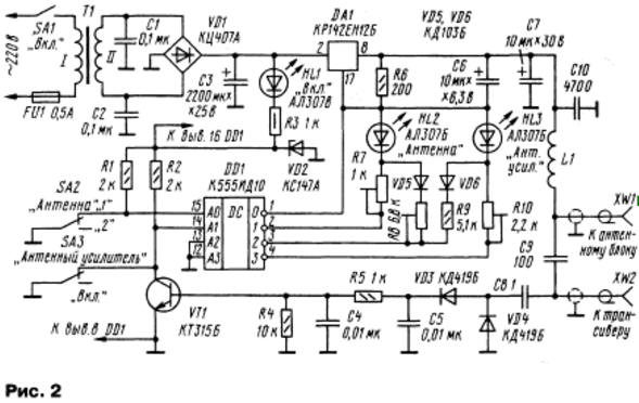
Encyclopedia of radio electronics and electrical engineering / Modernization of radio stations The diagram of the antenna unit is shown in fig. one.
It is placed close to the antennas. The unit is fed via a drop cable, and it is controlled by changing the supply voltage supplied to the XW3 socket and then through the L1 choke to the control unit (VT1-VT3) and to the UHF (VT4). If the supply voltage is absent or does not exceed 1,5V, the relays K1-KZ will be de-energized, and the transceiver is connected to antenna 1 (socket XW1) through their contacts. AU doesn't work. To connect antenna 2, a supply voltage of about 7 V is applied to the unit. At the same time, transistor VT2 opens, relay K1 is activated. In order to turn on the AU, a voltage of 11 or 15V is applied to the device. If the transceiver must work with antenna 2, a voltage of 11 V is applied. This will open the transistor VT3, the relays K2 and K3 will work and connect the AU. When switching to the transmission mode, the supply voltage is automatically reduced to 7 V and the AU is turned off. If the transceiver works with antenna 1, then when the AU is turned on, a voltage of 15 V is applied. The transistor VT1 will open, and VT2 will close. Relay K1 will be de-energized, so antenna 1 and AU will be connected. When switching to transmit mode, the supply voltage will decrease to 1.2V, so the AU will turn off (antenna 1 will remain connected). The AU is built on a low-noise left transistor and provides about 12 dB gain on the 430 MHz band with a bandwidth of about 10 MHz. At the input and output of the transistor, matching LC circuits on strip lines and protective diodes are installed. The supply voltage of the AU is stabilized by the DA1 chip. In the proposed version of the unit, an amplifier for the 430 MHz band is described, but instead of it, you can install a 144 MHz band amplifier by slightly changing the printed circuit board (see the article "Antenna amplifier for the 2-meter band" in "Radio", 2000, No. 1, p. 62, 63.) The power supply circuit is shown in fig. 2, and the algorithm of its operation is given in the table.
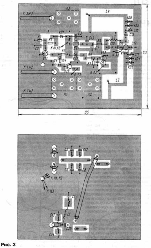
A rectifier with an output voltage of 1 ... 1 V is assembled on the transformer T3, the diode bridge VD23 and the capacitor C25. The DA1 microcircuit is a controlled voltage regulator. Diodes VD3 and VD4 - RF voltage detector. The unit is connected to the transceiver via connector XW2, and the drop cable is connected to XW1. The modes are switched by toggle switches SA2 and SA3. In the mode of operation with antenna 1 and the antenna amplifier turned off (as shown in Fig. 1 and Fig. 2), the decoder inputs have a low logic level, it is also present at the output O DD1, the output of the DA1 microcircuit is voltage 1,2 .XNUMX V. If you move the SA2 toggle switch to position "2", then a high level will go to the input of the AO decoder DD1. The decoder state will change, the output voltage of the unit will increase to 7 V and the HL2 LED will light up. Toggle switch SA3 includes AU. When switching to the RF transmission mode, the transceiver signal is rectified by the diodes VD3, VD4 and fed to the transistor VT1. It opens and sets the input A1 of the decoder to a low level. This will cause the AU to be disabled. In other words, the power supply allows you to independently switch antennas and turn on the AU. Most of the details of the antenna unit are placed on a printed circuit board made of double-sided foil fiberglass with a thickness of 1,5 mm, a sketch of which is shown in Fig. 3.
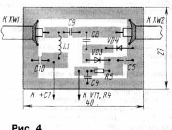
Both sides are connected to each other along the edge of the board with foil, in addition, they are connected through the holes in the board. The board is placed in a metal case, on one of the walls of which sockets XW1 -XW3 are installed. Nests must be used block-cable. In AC, transistors VT1-VT3 of the KT3102 series with letter indices A-E, KT312V, KT503B, KT503G can be used; VT4 - AP324A-2, AP324B-2, AP343A-2. The zener diode VD1 is any low-power one with a stabilization voltage of 14 ... 16 V, VD2 - 9 ... 11 V. In the 144 MHz range amplifier, the VD3-VD6 diodes can be replaced with KD522B. Trimmer capacitors - KT4-25, it is desirable to use constant K10-17 or other small-sized ones with leads of the minimum possible length. Relay K1-K3 - REK-43 with a response voltage of about 5 V. Chokes L1 and L3 are wound with wire PEV-2 0,4 on a mandrel with a diameter of 3 ... 3.5 mm and contain 8 ... 10 turns (12 ... 15 turns for the 144 MHz band). Setting up the device comes down to tuning the input and output circuits of the amplifier to the center frequency of the range. To increase the stability of the amplifier, it is recommended to apply a little absorbent material based on carbonyl iron to the drain terminal. The layout of the antenna unit had the following parameters: the insertion loss in the transmission mode was 0,35 (144 MHz) and 0,45 dB (430 MHz), and the SWR was 1,15 ... 1,2, respectively, and not more than 1,1. The attenuation of the signal from the unconnected antenna was -36 and -30 dB. In the power supply, the VT1 transistor can be replaced with a KT3102 with any letter index or a KT312 series transistor with indices A-B. Diode bridge VD1 - any with a permissible reverse voltage of at least 100 V and a current of at least 100 mA. LEDs can be used with any operating current up to 15 ... 20 mA and a voltage drop of not more than 3 V. Polar capacitors - K50-6, K50-16 or similar imported ones, the rest - K10-17, with C4, C5, C8- SU must have leads of a minimum length. Choke L1 is similar to the choke L1 of the antenna unit. Trimmer resistors - SPZ-19, constants - MLT, S2-33. Toggle switches SA1-SA3 - MT-1 or similar. Part of the parts of the power supply is placed on a printed circuit board made of double-sided foil fiberglass with a thickness of 1,5 mm, a sketch of which is shown in fig. 4.
Along the perimeter of the board, both sides are connected to each other with foil. The remaining parts can be mounted arbitrarily, including surface mounting. The DA1 chip must be placed on a heat sink with an area of about 100 cm2. Establishing a power supply comes down to setting the required values of the output voltage in accordance with the table. In this case, the transmitter signal can be simulated by installing a 10 kΩ resistor between the cathode of the zener diode VD2 and the base of the transistor VT1.
The world's tallest astronomical observatory opened
04.05.2024 Controlling objects using air currents
04.05.2024 Purebred dogs get sick no more often than purebred dogs
03.05.2024
▪ Bats' immunity to transmissible viruses explained ▪ Data transfer speed will double
▪ site section Computer devices. Article selection ▪ article by Johann Kaspar Lavater. Famous aphorisms ▪ article Who are sharks? Detailed answer ▪ article Chistyak spring. Legends, cultivation, methods of application ▪ Mustard article. Simple recipes and tips ▪ article Active RF switch. Encyclopedia of radio electronics and electrical engineering
Home page | Library | Articles | Website map | Site Reviews
www.diagram.com.ua |


 Leave your comment on this article: