|
|


 Arabic
 Bengali
 Chinese
 English
 French
 German
 Hebrew
 Hindi
Hindi Italian
 Japanese
 Korean
 Malay
Malay Polish
 Portuguese
 Spanish
 Turkish
 Ukrainian
 Vietnamese
|
ENCYCLOPEDIA OF RADIO ELECTRONICS AND ELECTRICAL ENGINEERING DSB transceiver. Encyclopedia of radio electronics and electrical engineering
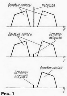
Encyclopedia of radio electronics and electrical engineering / Civil radio communications Before radio amateurs who have received permission to build a radio station of the fourth category, the question inevitably arises of making a simple KB transceiver. which would provide telephone operation on a range of 160 meters. In shortwave amateur radio, the vast majority of radio stations use single-sideband modulation (SSB) for telephone operation. However, due to the lack of experience, the manufacture of an SSB transceiver may not be within the power of beginner shortwaves. That is why the use of amplitude modulation (AM) is also allowed for radio stations of the fourth category. Receiving and transmitting equipment for this type of modulation is noticeably simpler, but the capabilities of AM radio stations are noticeably lower. Compared to SSB radios, they have a smaller "range", worse noise immunity. Moreover, the presence of a carrier frequency in the AM signal not only reduces the energy of the radio station (when powered from the mains, this is not very significant), but in a modern overcrowded air it inevitably leads to the appearance of specific interference - powerful interference "whistles". They occur due to beats between AM carriers of radio stations operating on adjacent frequencies. The solution to the problem "SSB is still difficult - AM is bad" can be the manufacture of a DSB transceiver as the first step in mastering single-sideband modulation. It differs from amplitude modulation DSB (Double Side Band - two-sideband modulation) by the absence of a carrier, which, by the way, contrary to its name, actually does not carry any information to the correspondent. And it differs from SSB in twice the band of the emitted signal - the band of the DSB signal is the same as that of AM. On fig. 1 shows the AM spectra. DSB and SSB signals (top to bottom). The carrier in DSB and SSB signals is typically attenuated by at least 40 dB. With this level of its suppression, interference due to interference between the remnants of carrier radio stations operating at adjacent frequencies is practically eliminated.
Essentially a DSB transceiver is a simplified SSB transceiver. which lacks the most expensive and difficult to manufacture and set up element (quartz or electromechanical filter). Moreover, the absence of a filter makes it possible to further simplify the transceiver by switching to "zero intermediate frequency" (direct frequency conversion). A description of just such a simple single-band DSB transceiver was published in the Japanese amateur radio "CO - ham radio" (1991, August, p. 312 - 317). This transceiver was made by the author for the 15 meters band, but without any problems it can be repeated on any other amateur KB band. A schematic diagram of the main unit of the transceiver is shown in fig. 2.
In the receive mode (supply voltage is applied to the "+ 12 V RX" bus, and the "+ 12 V TX" bus is connected to a common wire), the signal from the antenna is fed to the radio frequency amplifier on a field-effect transistor VT2. To ensure stable operation of the amplifier stage at radio frequencies, the drain circuit of the transistor is connected to part of the turns of the inductor L5. The diode VD1 in the receive mode is opened by the drain current of the transistor VT2 and does not affect the operation of this cascade. In the transmission mode, it will be practically closed, which will exclude the possible influence of the elements of the receiving path on the operation of the transmitting part of the transceiver (in particular, it will reduce the risk of self-excitation due to parasitic coupling through the antenna switch). The signal from the URF is fed to a balanced mixing detector on diodes VD2 - VD5. It is also supplied with high-frequency voltage from the local oscillator (VFO). The mixer is balanced by a trimmer resistor R12 and a trimmer capacitor C12. For receiving operation, the exact balancing of the mixing detector, generally speaking, is not very important, but when the same mixer works for transmission, it is very important. It is these tuning elements that achieve good suppression of the carrier frequency in the emitted signal. The detected signal is fed through a decoupling attenuator (resistors R9 - R11) and a low-pass filter (C14L7C15L8C16) with a cutoff frequency of about 2 kHz to an audio frequency preamplifier based on a VT3 field-effect transistor. The bias voltage for it is set by the attenuator resistors, since they are included in the DC source circuit of this transistor. Further amplification of the audio frequency signal is carried out by cascades on the operational amplifier DA I, transistor VT4 and chip DA3. These cascades do not have any features. The detector, assembled according to the scheme with doubling the voltage on the diodes VD6 and VD7, provides the AGC voltage. It is fed into the gate circuit of the transistor VT2. The PA1 microammeter indicates the change in the mode of this transistor under the influence of the AGC voltage, i.e., it acts as an indicator of the relative signal level (S-meter). In the absence of a signal, the trimmer resistor R8 sets the microammeter needle to zero division (SO). In transmission mode (supply voltage is applied to the "+12 V TX" bus, and the "+12 V RX" bus is connected to a common wire), the signal from the microphone through the level control on the variable resistor P23 and the low-pass filter (C32L9C33) is fed to the microphone amplifier on the operational amplifier DA2. The purpose of this low-pass filter is to exclude self-excitation of the transceiver in the transmit mode due to the passage of high-frequency interference to the microphone cable to the input of the microphone amplifier. After passing through the nodes common for the receiving and transmitting paths (low-pass filter - C14L7C15L8C16. attenuator - R9 - R11), the signal from the microphone amplifier goes to another common node - a mixer on diodes VD2 - VD5. The DSB signal generated in it is fed to the URF of the transmitting path, which is assembled on the transistor VT1 and is identical to the URF of the receiving path, and from it to the power amplifier. The local oscillator circuit is shown in fig. 3. It consists of a master oscillator on a transistor VT1 and a buffer amplifier stage on a transistor VT2. The master oscillator is made according to the well-known "capacitive three-point" scheme, and the buffer stage is identical to the cascades of the main unit (see Fig. 2). The supply voltage of the master oscillator +5 V is stabilized by the DA1 chip.
When repeating the design, transistors VT1 - VT2 in the main node and in the local oscillator node can be replaced by KP303E. To increase the sensitivity of the receiving path of the transceiver, the author used a VT3 transistor with low intrinsic noise (possible replacement - KP303A-B). However, on a range of 160 meters, a transistor with non-normalized noise (the same KP303E) can also be used here. The presence of URF in the receiving path and the high level of terrestrial noise in this range reduce the requirements for the noise characteristics of the ultrasonic frequency. The DA1 and DA2 microcircuits have a complete analogue of domestic production - K140UD7, but many other general-purpose operational amplifiers can also be used here. Transistor VT4 can be almost any low power and npn structure. starting from KT315, with a static current transfer coefficient of at least 50. The OAZ microcircuit has no analogue of domestic production, but this is the most common ultrasonic frequency converter. therefore, this cascade can be replaced with any ultrasonic frequency converter (for example, with K174UN7 in a typical inclusion). Diodes VD1 - VD6 - any high-frequency silicon (KD503 and the like). The inductance of the low-pass filter coils of the main assembly L7 and L8 is 3 mH, which, with the values of capacitors C14-C16 indicated in the diagram, provides a filter cutoff frequency of about 2 kHz. The inductance of the coil L9 of the low-pass filter of the microphone amplifier is 390 μH, but the use here of coils with an inductance that differs from that indicated by one and a half to two times 8 on one side or the other will not affect the device's performance. The same applies to the L2 inductor in the local oscillator node. Inductance coils L2. L4, L5 (main node) and L1, L3 (local oscillator node), as well as the capacitances of the capacitors connected in parallel to them, depend on which range the transceiver will be manufactured for. Communication coils should have about ten times fewer turns than the coils connected to them oscillatory circuits. Capacitors C34 and C21 serve to limit the bandwidth of the UZCH in the receiving path and the microphone amplifier in the transmitting path. Their capacitance can lie in the range of 200 ... 500 pF. In principle, these capacitors can not be installed. The integral stabilizer DA1 in the local oscillator node can be replaced with similar products from the K142 series or with the most common one - with a zener diode.
Machine for thinning flowers in gardens
02.05.2024 Advanced Infrared Microscope
02.05.2024 Air trap for insects
01.05.2024
▪ New DACs from TI - high precision and low consumption ▪ Home appliances will determine when the owners are sleeping ▪ IDrive One external drive with 802.11ac Wi-Fi adapter
▪ section of the site Winged words, phraseological units. Selection of articles ▪ article With fat to rage. Popular expression ▪ article Have people always lived in families? Detailed answer ▪ article Electric floor polishers. Encyclopedia of radio electronics and electrical engineering
Home page | Library | Articles | Website map | Site Reviews
www.diagram.com.ua |


 Leave your comment on this article: