|
|


 Arabic
 Bengali
 Chinese
 English
 French
 German
 Hebrew
 Hindi
Hindi Italian
 Japanese
 Korean
 Malay
Malay Polish
 Portuguese
 Spanish
 Turkish
 Ukrainian
 Vietnamese
|
ENCYCLOPEDIA OF RADIO ELECTRONICS AND ELECTRICAL ENGINEERING Powerful laboratory power supply with OU. Encyclopedia of radio electronics and electrical engineering
Encyclopedia of radio electronics and electrical engineering / Power Supplies There is probably no radio amateur who did not have a laboratory power supply as one of the first designs. When making experiments, making individual devices, every radio amateur is sure to face the problem of power supply. It happens that, having made a power supply for any design, while spending a lot of time and money searching for a suitable circuit and details in the literature, a novice designer is convinced that his device does not work well with this unit. This often happens with those radio amateurs who, without a laboratory source, cannot correctly determine either the range of supply voltages at which their devices work stably, or the currents they practically consume. It is necessary to do this during the adjustment of devices, feeding them from an external source, which would provide wide limits for adjusting the output voltage and its high stability with large changes in load current. In addition, such a source must have high-speed protection against overload or output short circuits. The popular radio technical literature constantly highlights the design of power supplies and repeatedly describes noteworthy laboratory sources. However, some of them either provide insufficient load current with other excellent parameters, or contain a number of scarce parts, or are difficult to configure. Therefore, their repetition is not available to every radio amateur, especially a beginner. The efficiency of the described power supply, like most similar devices, does not exceed 50%. When repeated, you will have to work hard on winding the power transformer. However, the relative simplicity of the circuit with sufficiently high output parameters, the gain in tuning, weight and dimensions gives certain advantages. The main characteristics of the power supply:
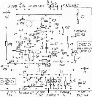
The power supply (Fig. 1) consists of a main compensation stabilizer with a serial connection of a regulating element (transistors VT2-VT4), an amplifier in the feedback circuit (microcircuit DA1, transistor VT1), auxiliary parametric stabilizers (zener diodes VD11-VD14, VD19) and a device overload protection (transistors VT5, VT6). In compensation stabilizers, the output voltage is the difference between the voltage coming from the rectifier and the voltage drop across the regulating transistor.
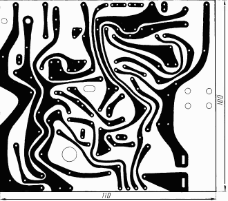
The desire to design a stabilizer with a smooth change in the output voltage over a wide range and a significant load current is associated with the release of large thermal power on the regulating transistor. For this reason, a step change in the rectified voltage is used in the block. To do this, the main rectifier, made on diodes VD2-VD5, is supplied with voltage from the sectioned secondary winding III of the power transformer using the SA2.1 section of the SA2 switch. At the same time switch SA2 (sections SA2.2 and SA2.3) switches the resistors of the control stages of the stabilizer. In this case, the output voltage can be changed in ten steps of 3 V and smoothly using resistor R41 within each step. As a result, at the maximum load current on the main regulating transistor VT2-VT4, connected according to the common collector circuit, power is dissipated no more than 20 watts. Transistors VT3 and VT4 are connected in parallel and, accordingly, the power dissipated on each of them does not exceed 10 watts. The emitters of these transistors include resistors R42 and R43, which serve to equalize their currents. To reduce the overall dimensions and weight of the power supply, increase the compactness of the installation, a radiator with a smaller than necessary scattering area was used. At the same time, transistors are heated up to 60 ... 70 ° C during long-term operation of the power supply at the maximum load current. If the power supply is supposed to operate for a long time at load currents close to the maximum, then a radiator with a dissipation area of 800 ... 1000 cm2 should be used. The feedback signal amplifier is assembled on an operational amplifier (op-amp) DA1, which is powered by an auxiliary rectifier made on VD6-VD9 diodes. The supply voltage of the op-amp is stabilized by two parametric stabilizers connected in series, the first of which is made on zener diodes VD11, VD12 and resistor R3, and the second on zener diodes VD13, VD14 and resistor R4. The voltage stabilized by the VD14 zener diode is also used to power the reference voltage source, which is made on the VD19 zener diode, which has a low stabilization voltage temperature coefficient, and resistor R21. By changing the reference voltage supplied to the inverting input of the op-amp using the divider R22-R41, you can change the voltage of the stabilizer. To obtain the output voltage of the power supply, which exceeds the maximum output voltage of the op-amp, an amplifier on the transistor VT1 is used. Resistor R11 limits the output current of the op-amp. Through a divider on resistors R19, R20, part of the output voltage of the unit is fed to the non-inverting input of the op-amp. With any random change in the output voltage of the stabilizer, the difference between the voltages at the inputs of the op-amp changes and, accordingly, the voltage at the collector VT1, which changes the state of the regulating transistor in such a way that the output voltage of the unit returns to its previous value. Capacitors C5-C7, C9, C10 eliminate block self-excitation at high frequencies over the entire range of output voltage and load current. To ensure the output voltage of the power supply close to 0, the bases of the transistors VT3, VT4 are supplied through the resistor R8 with a closing voltage formed by the divider current R6, R7 across the resistor R7. In the absence of this voltage, it would not be possible to obtain the output voltage of the unit less than 1 ... 1,5 V. The reason for this is the final value of the collector current of transistors VT2-VT4 at zero voltage at their bases. The VD17R14 circuit is used to accelerate the discharge of the capacitor C12 and the capacitive load connected to the unit while setting a lower unit output voltage level. In this case, the capacitor C12 is discharged to the voltage established on the collector of the transistor T1 along the circuit: the positive terminal of the capacitor C12, the resistor R12, the emitter-collector junction of the transistor VT1, the diode VD17, the resistor R14, the negative terminal of the capacitor C12. The electronic overcurrent protection device is made on transistors VT5, VT6. The voltage drop created by the load current across the resistor R12, in the opening polarity, is applied to the emitter junction of the transistor VT5. At the same time, the closing voltage from resistor R15, regulated by resistor R17, is supplied to the same transition. As soon as the load current exceeds the specified level, VT5 opens slightly, opening the transistor VT6. The latter, in turn, will open VT5 even more - the process proceeds like an avalanche. As a result, both transistors are fully opened and a negative polarity signal is supplied to the input 10 of the op-amp through the diode VD18 and resistor R18, which exceeds the signal at input 9 in absolute value. A negative polarity voltage is generated at the output of the op-amp, opening the transistor VT1. In this case, the regulating element (transistors VT2-VT4) closes, and the output voltage of the unit becomes close to 0. At the same time, the signal lamp H2 "Overload" lights up. To return the block to its original state, you need to turn it off for a few seconds and turn it on again. The winding IV of the power transformer, the auxiliary rectifier on the diode VD1, the capacitor C1 and the diode VD10 serve to eliminate the appearance of an increased voltage at the output of the unit from the main rectifier when the power supply is turned off. This is possible because capacitor C2 discharges faster than capacitor C3. In this case, the supply voltage of the op-amp disappears faster, and, therefore, the transistor VT1 is locked, and the control element is unlocked before the voltage across the capacitor C3 disappears. The positive terminal of the capacitor C3 through the emitter junction of the transistor VT1 is connected to the anode of the diode VD10, but the diode does not affect its operation when the power supply is on, since it is closed by a positive voltage formed by the difference between the voltage across the capacitor C3 and the voltage across the capacitor C1. The latter is always greater due to the charging of the capacitor C1 by the sum of the output voltages of the windings III and IV of the power transformer. To ensure this condition, it is necessary to observe the polarity of the inclusion of windings III and IV such as shown in the diagram. After turning off the power supply, capacitor C1 quickly discharges through resistor R1, diode VD10 opens with voltage across capacitor C3, and the latter through resistor R1 enters the base of transistor VT1. Transistor VT1 is unlocked, closing the control element. In this case, the load voltage is maintained close to zero, until the capacitor C3 is completely discharged through the transistor VT1 and resistor R9. Resistor R2 accelerates the discharge of capacitor C2 and eliminates the surge in the output voltage of the unit at the very initial moment when it is turned off, while capacitor C1 has not yet had time to discharge and diodes VD10 and transistor VT1 have not opened. The appearance of a surge at this moment is associated with an unequal change in the voltages at the inputs of the op-amp and the appearance of a positive jump at its output. Capacitor C4, resistor R5 and diode VD16 are used to eliminate the surge of output voltage when the power supply is turned on, as well as to prevent the protection from tripping with a significant capacitive load at the moment of switching on. At the initial moment after switching on, the capacitor C4 is slowly charged in two circuits: through the resistor R5 and through the resistor R9 and the diode VD16. In this case, the voltage at the base of the transistor VT2 is equal to the sum of the voltage drop across the open diode VD16 and the voltage across the capacitor C4. This voltage, and hence the voltage at the output of the power supply will grow following the voltage across the capacitor C4 until the stabilizer enters a steady state. Next, the VD16 diode closes, and the capacitor C4 is charged only through the resistor R5 to the maximum voltage on the filter capacitor C3 and does not have any effect on the further operation of the power supply. Diode VD15 serves to accelerate the discharge of capacitor C4 when the unit is off. All elements, except for the power transformer, powerful control transistors, switches SA1-SA3, fuse holders FU1, FU2, light bulbs H1, H2, pointer meter, output connectors and a smooth output voltage regulator, are placed on printed circuit boards (Fig. 2).
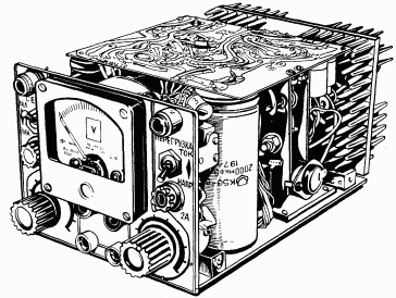
The location of the elements is shown in Fig. 3., the appearance of the power supply - in Fig. 4.
The P210A transistors are mounted on a needle-shaped heatsink mounted at the back of the case and having an effective dissipation area of about 600 cm2. Ventilation holes with a diameter of 8 mm are drilled in the bottom of the case at the place where the radiator is attached. The housing cover is fixed in such a way that an air gap of about 0,5 cm wide is maintained between it and the radiator. For better cooling of the control transistors, it is recommended to drill ventilation holes in the cover. A power transformer is fixed in the center of the case, and next to it, on the right side, a P5A transistor is fixed on a 2,5x214 cm duralumin plate. The plate is insulated from the body with insulating bushings. The diodes KD202V of the main rectifier are mounted on duralumin plates screwed to the printed circuit board. The board is installed above the power transformer with the parts down. The power transformer is made on a toroidal tape magnetic circuit OL 50-80/50. The primary winding contains 960 turns of wire PEV-2 0,51. Windings II and IV have output voltages of 32 and 6 V, respectively, with a voltage on the primary winding of 220 V. They contain 140 and 27 turns of wire PEV-2 0,31. Winding III is wound with PEV-2 1,2 wire and contains 10 sections: the lower one (according to the diagram) - 60, and the rest 11 turns each. The output voltages of the sections are respectively equal to 14 and 2,5 V. The power transformer can also be wound on another magnetic circuit, for example, on a rod from TVs UNT 47/59 and others. The primary winding of such a transformer is retained, and the secondary windings are rewound to obtain the above voltages. In the power supply, instead of transistors P210A, you can use transistors of the P216, P217, P4, GT806 series. Instead of P214A transistors, any of the P213-P215 series. MP26B transistors can be replaced with any of the MP25, MP26 series, and P307V transistors with any of the P307 - P309, KT605 series. Diodes D223A can be replaced by diodes D223B, KD103A, KD105; diodes KD202V - any powerful diodes with a permissible current of at least 2 A. Instead of the D818A zener diode, you can use any other zener diode from this series. Switches SA2 - small-sized biscuit type 11P3NPM. In the second block, the contacts of the two sections of this switch are paralleled and are used to switch sections of the power transformer. When the power supply is on, the position of the switch SA2 should be changed at load currents not exceeding 0,2 ... turning it off. Variable resistors for smooth adjustment of the output voltage should be selected with the dependence of resistance on the angle of rotation of the type "A" engine and preferably wire. Miniature incandescent bulbs HCM-0,3 V-1 mA are used as signal lamps H2, H9. Any pointer device can be used for a current of full deflection of the pointer up to 1 mA and a front part size of not more than 60X60 mm. In this case, it must be remembered that the inclusion of a shunt in the output circuit of the power supply increases its output impedance. The greater the current of the total deviation of the arrow of the device, the greater the resistance of the shunt (provided that the internal resistances of the devices are of the same order). To prevent the influence of the device on the output impedance of the power supply, the switch SA3 during operation should be set to measure voltage (upper position according to the diagram). In this case, the shunt of the device closes and is excluded from the output circuit. Establishing the power supply comes down to checking the correctness of the installation, selecting the resistors of the control stages to adjust the output voltage within the required limits, setting the protection operation current and selecting the resistances of the resistors Rsh and Rd for the pointer meter. Before setting up the power supply, a short wire jumper is soldered instead of a shunt. When setting up the unit, it is connected to the network, the switch SA2 and the slider of the resistor R41 (see Fig. 1) are set to the position corresponding to the maximum output voltage (upper position according to the diagram). Then, by selecting the resistor R22, the voltage at the output of the power supply is set to 30 V. The variable resistor R41 can also be used with a different value within 51 ... 120 Ohms. In this case, the nominal resistance of the resistors R23-R40 is selected 5 ... 10% less than the resistance of the resistor R41. Next, configure the protective device. To do this, solder one of the terminals of the VD18 diode and connect a resistor with a resistance of 5 ... 10 ohms with a power of at least 25 watts to the output of the block. Then the output voltage of the unit is set so that the current through the resistor controlled by the external device is 2,5 A. By adjusting the resistor R17, the protection is activated at this current. After completing the setup, solder the VD18 diode in place. For reliable operation of the protection at the minimum mains voltage, a resistor R16 is selected. An avalanche-like process depends on it, leading to the unlocking of transistors VT5 and VT6. When repeating the power supply, it should be borne in mind that the wire coming from the resistor R24 to the common wire must be connected directly to the printed circuit board, and not to the terminals of the Rsh shunt or the PA1 pointer meter. Otherwise, when the load is connected, the output voltage of the unit may increase. This increase can reach 0,3 ... 0,5 V at the maximum load current, depending on the length and diameter of the wire connecting the connection point of the resistors R12, R20 with the connection point of the capacitor C 12 and shunt Rsh. This happens because the voltage drop that forms on the wires from the load current is applied in series with the reference voltage to the inverting input of the op-amp. A piece of manganin or constantan wire with a diameter of 1 mm is used as a shunt. When setting up the shunt, switch SA3 is switched to the "current" position, and the power supply is turned on only after a piece of manganin wire is soldered instead of the previously installed jumper. Otherwise, the pointer meter PA1 may fail. In this case, the external device is connected in series with the load, which can be a 5 ... 10 Ohm resistor designed for a dissipation power of 10 ... 50 W. By changing the output voltage of the power supply, the load current is set to 2 ... 2,5 A and, by reducing or increasing the length of the manganin wire, the same readings of the PA1 meter are achieved. Before each operation to change the length of the shunt, do not forget to turn off the power supply.
Machine for thinning flowers in gardens
02.05.2024 Advanced Infrared Microscope
02.05.2024 Air trap for insects
01.05.2024
▪ Power transistors StrongIRFET2 ▪ Phison PS5.0-E5026 PCIe 26 Drive ▪ NXP is preparing an ultra-compact Wi-Fi chip ▪ Nokia CDMA phone with GPS module
▪ section of the site Voltage stabilizers. Article selection ▪ article Whispers, timid breathing, nightingale trills. Popular expression ▪ article Which Olympic champion did not know she was participating in the Olympics? Detailed answer ▪ article Common pear. Legends, cultivation, methods of application
Home page | Library | Articles | Website map | Site Reviews
www.diagram.com.ua |


 Leave your comment on this article: