|
|


 Arabic
 Bengali
 Chinese
 English
 French
 German
 Hebrew
 Hindi
Hindi Italian
 Japanese
 Korean
 Malay
Malay Polish
 Portuguese
 Spanish
 Turkish
 Ukrainian
 Vietnamese
|
ENCYCLOPEDIA OF RADIO ELECTRONICS AND ELECTRICAL ENGINEERING Quasi-resonant voltage converter. Encyclopedia of radio electronics and electrical engineering
Encyclopedia of radio electronics and electrical engineering / Power Supplies The article tells about a very promising type of voltage converter - quasi-resonant. The described device provides an exceptionally high conversion efficiency, allows the output voltage to be regulated and stabilized, and operates stably with varying load power. In modern network power supplies - various equipment, transistorized voltage converters are widely used. Their advantages over transformer blocks are well known - smaller dimensions and reduced copper consumption at the same output power, which more than pays for their complexity, especially in mass production. The higher the operating frequency of the conversion, the higher its economic performance. However, with an increase in the switching frequency of transistors, switching losses also increase and, accordingly, the efficiency of the converter decreases. The value of switching losses of any converter is determined mainly by two factors - the presence of a through current and a significant closing time of powerful switching transistors at a large collector current. Their opening time, as a rule, is seven to ten times less and does not significantly affect the efficiency. Through current occurs when switching transistors in bridge and half-bridge converters. It flows at a time when the transistor of one arm of the converter is already open, and the other has not yet had time to close. To eliminate this phenomenon, the switching process is divided into two stages. First, the transistor is closed in one of the arms, and then, after 3 ... 5 μs (typical closing time of powerful transistors), it is opened in the other. This method is used in converters with external excitation, but it is not applicable in self-oscillating ones. Long-term closing at a high collector current leads to the fact that at this time, useless power is released on the closed transistor, the average value of which is expressed by the formula: P=Im*Um*F*tclose/6, where Im is the collector current of the transistor at the beginning of its closing;
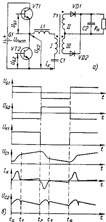
There are various schemes that allow you to speed up the closing process, but they require additional energy costs and reduce the closing time, at best, no more than two times from the passport, and often only help to stay at this value. In addition to switching, there are power losses due to a voltage drop across an open transistor, but they depend only on the choice of transistors and in network converters do not exceed 0,5 ... 1% of the converted power. The whole variety of existing voltage converters, both with external excitation and autogenerator ones, can be conditionally divided into several types according to the nature of the collector current and voltage at the moment of switching. The first and most common is pulsed, which is characterized by the maximum collector current by the time the transistors are closed and the maximum collector voltage after. In such a converter, both components of switching losses act, therefore, at an operating frequency of 15 ... 25 kHz, they account for 8 ... 15% of the converted power. Despite this, pulse converters are the most common due to the ease of implementation and flexibility in controlling the output voltage, which makes it possible to combine voltage conversion with its stabilization. The second type is a resonant converter. A simplified example of this is a conventional LC oscillator with transformer feedback and an automatic bias circuit. The reactive elements of the collector circuit are calculated so that either before closing the transistor, its collector current decreases to almost zero, or immediately after closing, the collector voltage is very small. This allows reducing the total losses on switching transistors to 1 ... 2% of the converted power and reducing the level of radio interference compared to a pulse converter. However, resonant converters work reliably only in the autogenerator mode, they do not allow the possibility of regulating the output voltage and a significant deviation of the load resistance from the calculated value. In general, in the converter-stabilizer system, they lose to impulse ones in terms of efficiency, since they require a separate stabilizer. The third type is interesting and undeservedly little widespread - quasi-resonant, which is largely spared from the shortcomings of both previous ones. The idea of creating such a converter is not new, but practical implementation became feasible relatively recently, after the advent of powerful high-voltage transistors that allow a significant collector pulse current at a saturation voltage of about 1,5 V. The main distinguishing feature and the main advantage of this type of power supply is the high efficiency of the voltage converter, reaching 97 ... 98% without taking into account losses in the rectifier of the secondary circuit, which are mainly determined by the load current. The high efficiency in some cases generally eliminates the need to use heat sinks for powerful converter transistors, which makes it possible to significantly reduce the size of the equipment, not to mention other economic advantages. From a conventional pulse converter, in which, by the time the switching transistors are closed, the current flowing through them is maximum, the quasi-resonant one differs in that by the time the transistors are closed, their collector current is close to zero. Moreover, a decrease in current by the time of closing is provided by the reactive elements of the device. It differs from the resonant one in that the conversion frequency is not determined by the resonant frequency of the collector load. Due to this, it is possible to regulate the output voltage by changing the conversion frequency and implement the stabilization of this voltage. Let us explain in more detail the principle of operation of a half-bridge quasi-resonant converter using a simplified diagram shown in Fig. 1a. Diagrams of current and voltage at characteristic points in the steady state operation are shown in fig. 1b. For simplicity, let's assume that the switching time of the transistors is infinitesimal; this simplification, as practice has shown, does not affect the reliability of the diagrams.
We also assume that the values of the parameters of the elements satisfy the relations: LT>>L1 and Fpt Consideration will begin from the moment to, when the transistor VT1 opens and through it, as well as through the inductor L1 and the primary winding of the transformer T1, the capacitor C1 begins to charge. At this moment, the voltage on the capacitor C2 and the load Rn is less than the voltage (Upit-Uc1)n-UD, where Uc1 is the voltage on the capacitor C1; n is the transformation ratio of the transformer T1; UD - direct voltage drop across the rectifier diode VD1 (or VD2). In this case, the diode VD1 is open and the charging current of the capacitor C2 passes through it. When charging, the capacitor C2 shunts the secondary winding of the transformer T1, so the charging rate of the capacitor C1 is determined by its own capacitance and the low inductance of the inductor L1 and does not depend on the inductance of the primary winding of the transformer. Since, as the capacitor charges, the voltage on the primary winding decreases, and on the capacitor C2 increases, then at the moment t, the diode VD1 closes and a large inductance of the primary winding of the unloaded transformer T1 is included in the charging circuit of the capacitor C1. In this case, the current through the open transistor VT1 abruptly decreases to the value of the current in the primary winding, which is still insignificant at this point, since Lt>>L1. Thus, from the moment t1 until the moment of switching of the transistors t2, the increase in the collector current is determined by the inductance of the primary winding of the unloaded transformer, which is chosen quite large. In fact, the state of the circuit at the time of switching corresponds to the idle mode. In real circuits, the role of the choke L1 can be performed by the leakage inductance of the transformer. After closing the transistor VT1 and opening VT2, the capacitor C1 is discharged. The current through the inductor and winding I of the transformer flows in the opposite direction, but the processes follow the same laws. A necessary condition for the existence of the described mode is that the rate of voltage decrease on the capacitor C2 when it is discharged through the load resistance after closing the diodes must be less than the rate of voltage decrease on the primary winding of the transformer in the same period of time, then the rectifier diodes remain closed until the next switching transistors. To ensure minimum power loss, the forward voltage drop across the open transistor must be minimal at any allowable collector operating current. However, to maintain the maximum current for this base throughout the entire half-cycle of this transistor is energetically unfavorable, and there is no need for this. It is enough to ensure that the base current is proportional to the collector current; such control is called proportional-current.
Since the reactive elements reduce the collector current to a minimum by the time the transistor closes, the base current will also be minimal and, therefore, the closing time of the transistor is reduced to the value of the opening time. Thus, the problem of through current that occurs during switching is completely removed. In other words, the use of the quasi-resonant mode together with proportional-current control makes it possible to almost completely get rid of switching losses. Two practical options for a mains power supply with a quasi-resonant converter and current proportional control are described below. The manufacture of these blocks will not cause great difficulties for radio amateurs and will allow you to evaluate all the advantages of the converter. The stabilized unit has been operating in a high-frequency frequency counter for more than two years and does not cause any complaints. On fig. 2 shows a schematic diagram of a self-generating unstabilized power supply.
The main share of power losses in the unit falls on the heating of the rectifier diodes of the secondary circuit, and the efficiency of the converter itself is such that there is no need for heat sinks for transistors. The power loss on each of them does not exceed 0,4 W. Special selection of transistors for any parameters is also not required. When the output is closed or the maximum output power is exceeded, the generation is interrupted, protecting the transistors from overheating and breakdown. The filter, consisting of capacitors C1-C3 and inductor L1L2, is designed to protect the power supply from high-frequency interference from the converter. The start of the oscillator is provided by the R4C6 circuit and the capacitor C5. Oscillations are generated as a result of the action of a positive feedback through the transformer T1, and their frequency is determined by the inductance of the primary winding of this transformer and the resistance of the resistor R3 (with increasing resistance, the frequency increases). Winding IV of the transformer T1 is designed for proportional-current control of transistors. It is easy to see that the powerful isolating transformer T2 and the control circuits of switching transistors (transformer T1) are separated, which makes it possible to significantly weaken the influence of parasitic capacitance and inductance of transformer T2 on the formation of the base current of transistors. Diodes VD5 and VD6 limit the voltage across the capacitor C7 at the moment the converter is started, while the capacitor C8 is charged to the operating voltage. When setting up the device, it is necessary to make sure that the converter operates in a quasi-resonant mode. To do this, a temporary resistor with a resistance of 7 ... 1 ohms with a power of 3 W is connected in series with the capacitor C2 and, having applied a signal from this resistor to the input of the oscilloscope, the shape of the collector current pulses of both transistors is observed on the screen at maximum load. These should be bipolar alternating bell-shaped pulses that do not overlap in time. If they overlap, it is necessary to reduce the inductance of the inductor L3 by unwinding 10 ... 15% of the turns, or to reduce the generation frequency of the converter by selecting the resistor R3. Note here that not all oscilloscopes allow measurements in circuits that are not galvanically isolated from the mains. The inductor L1L2 and the transformer T1 are wound on the same ring magnetic cores K12x8x3 from 2000NM ferrite. The inductor windings are performed simultaneously, "in two wires", with a PELSHO 0,25 wire; the number of turns is 20. Winding I of the transformer T1 contains 200 turns of wire PEV-2 0.1, wound in bulk, evenly throughout the ring. Windings II and III are wound "in two wires" - 4 turns of wire PELSHO 0,25; winding IV is a coil of the same wire. For the T2 transformer, a K28x16x9 ring magnetic circuit made of 3000NN ferrite was used. Winding I contains 130 turns of PELSHO 0,25 wire, laid turn to turn. Windings II and III - 25 turns of wire PELSHO 0,56 each; winding - "in two wires", evenly around the ring. The inductor L3 contains 20 turns of PELSHO 0,25 wire wound on two ring magnetic cores K12x8x3 of 2000NM ferrite folded together. Diodes VD7, VD8 must be installed on heat sinks with a dissipation area of at least 2 cm2 each.
The described device was designed to be used in conjunction with analog regulators for various voltage values, so there was no need for deep ripple suppression at the output of the unit. Ripple can be reduced to the required level by using the usual LC filters in such cases, such as, for example, in the block described below. The scheme of a stabilized power supply based on a quasi-resonant converter is shown in fig. 3. The output voltage is stabilized by appropriately changing the operating frequency of the inverter.
As in the previous block, powerful transistors VT1 and VT2 do not need heat sinks. Symmetrical control of these transistors is implemented using a separate master pulse generator assembled on a DD1 chip. Trigger DD1.1 works in the actual generator. The pulses have a constant duration set by the R7C12 circuit. The period is changed by the OS circuit, which includes the optocoupler U1, so that the voltage at the output of the block is maintained constant. The minimum period sets the chain R8C13. Trigger DD1.2 divides the repetition frequency of these pulses by two, and the square wave voltage is supplied from the direct output to the transistor current amplifier VT4VT5. Further, the current-amplified control pulses differentiate the R2C7 circuit, and then, already shortened to a duration of approximately 1 μs, they enter through the transformer T1 into the base circuit of the transistors VT1, VT2 of the converter. These short pulses serve only to switch transistors - closing one of them and opening another. The base current of the transistor opened by the control pulse supports the action of a positive current feedback through the winding IV of the transformer T1. Resistor R2 also serves to dampen parasitic oscillations that occur at the moment of closing the rectifier diodes of the secondary circuit in the circuit formed by the interturn capacitance of the primary winding of the transformer T1, the inductor L3 and the capacitor C8. These parasitic oscillations can cause uncontrolled switching of transistors VT1, VT2. The described version of the converter control allows you to keep the proportional current control of the transistors and at the same time adjust the frequency of their switching in order to stabilize the output voltage. In addition, the main power from the excitation generator is consumed only at the moments of switching of powerful transistors, so the average current consumed by it is small - does not exceed 3 mA, taking into account the current of the Zener diode VD5. This allows it to be powered from the primary circuit through the quenching resistor R1. Transistor VT3 works as a control signal voltage amplifier, just like in a compensation stabilizer. The coefficient of stabilization of the output voltage of the block is directly proportional to the static current transfer coefficient of this transistor. The use of a transistor optocoupler U1 provides reliable galvanic isolation of the secondary circuit from the mains and high noise immunity at the master oscillator control input. After the next switching of transistors VT1, VT2, the capacitor C10 begins to recharge and the voltage at the base of the transistor VT3 begins to increase, the collector current also increases. As a result, the optocoupler transistor opens, maintaining the master oscillator capacitor C13 in a discharged state. After closing the rectifier diodes VD8, VD9, the capacitor C10 begins to discharge to the load and the voltage across it drops. The transistor VT3 closes, as a result of which the charging of the capacitor C13 begins through the resistor R8. As soon as the capacitor is charged to the switching voltage of the trigger DD1.1, a high voltage level will be set at its direct output. At this moment, the next switching of transistors VT1, VT2 takes place, as well as the discharge of the capacitor C13 through the opened transistor of the optocoupler. The next process of recharging the capacitor C10 begins, and the trigger DD1.1 after 3 ... 4 μs will again return to the zero state due to the small time constant of the R7C12 circuit, after which the entire control cycle is repeated, regardless of which of the transistors - VT1 or VT2 - open in the current half-cycle. When the source is turned on, at the initial moment, when the capacitor C10 is completely discharged, there is no current through the optocoupler LED, the generation frequency is maximum and is determined in the main time constant of the R8C13 circuit (the time constant of the R7C12 circuit is several times less). With the ratings of these elements indicated on the diagram, this frequency will be about 40 kHz, and after dividing it with a DD1.2 trigger, it will be 20 kHz. After charging the capacitor C10 to the operating voltage, the OS stabilizing loop on the elements VD10, VT3, U1 comes into operation, after which the conversion frequency will already depend on the input voltage and load current. Voltage fluctuations on the capacitor C10 smoothes the filter L4C9. Chokes L1L2 and L3 are the same as in the previous block. Transformer T1 is made on two ring magnetic cores K12x8x3 of 2000NM ferrite folded together. The primary winding is wound in bulk evenly over the entire ring and contains 320 turns of wire PEV-2 0,08. Windings II and III contain 40 turns of wire PELSHO 0,15; they are wound "in two wires". Winding IV consists of 8 turns of PELSHO 0,25 wire. Transformer T2 is made on a K28x16x9 ring magnetic circuit made of 3000NN ferrite. Winding 1-120 turns of wire PELSHO 0,15, and II and III - 6 turns of wire PELSHO 0,56, wound "in two wires". Instead of the PELSHO wire, you can use the PEV-2 wire of the appropriate diameter, but at the same time, two or three layers of varnished cloth must be laid between the windings. Inductor L4 contains 25 turns of PEV-2 0,56 wire wound on a K12x6x4,5 ring magnetic circuit made of 100NN1 ferrite. Any ready-made choke with an inductance of 30 ... 60 μH for a saturation current of at least 3 A and an operating frequency of 20 kHz is also suitable. All fixed resistors are MLT. Resistor R4 - trimmer, any type. Capacitors C1-C4, C8 - K73-17, C5, C6, C9, C10-K50-24, the rest - KM-6. The KS212K zener diode can be replaced with KS212Zh or KS512A. Diodes VD8, VD9 must be installed on radiators with a dissipation area of at least 20 cm2 each. To establish the unit, it is necessary to connect a temporary resistor with a resistance of 1 kOhm with a power of 1-0,25 W in parallel with the resistor R1 and, without connecting the load, apply a constant or alternating voltage with an amplitude of 15 ... 20 V to the input of the block, and a constant voltage of 5 V to the output in the correct polarity. Set the slider of the resistor R4 to the lower position according to the diagram. The Y input of the oscilloscope is connected to the collector and emitter of the transistor VT2. On the screen, rectangular pulses with a duty cycle of 2 ("meander") with an amplitude of 14 ... 19 V and a frequency of 20 kHz should be visible. If, when the slider of the resistor R4 is moved upwards, the frequency decreases and then the oscillations stall, then the stabilization unit is working normally. Having set the frequency within 4 ... 3 kHz with resistor R5, turn off the power from the input and output, remove the temporary resistor. A load equivalent is connected to the output of the block, and the input is connected to the network, and the output voltage is set by resistor R4. The efficiency of both blocks can be increased if Schottky diodes are used instead of KD213A diodes, for example, any of the KD2997 series. In this case, heat sinks for the diodes are not required. References:
Author: E.Konovalov
Machine for thinning flowers in gardens
02.05.2024 Advanced Infrared Microscope
02.05.2024 Air trap for insects
01.05.2024
▪ Using rain to reduce air pollution ▪ The popularity of ultraportable laptops is growing ▪ Extra strong glass LionGlass
▪ site section Frequency synthesizers. Selection of articles ▪ article by Milton Friedman. Famous aphorisms ▪ article Zopnik prickly. Legends, cultivation, methods of application ▪ article Lamp-book. Encyclopedia of radio electronics and electrical engineering ▪ article A flower that changes color. Focus Secret
Comments on the article: Alexander Belomestnykh I collected this converter once upon a time. The only problem is it won't start. To start, I had to add a circuit on a kt315g transistor. And so the scheme works.
Home page | Library | Articles | Website map | Site Reviews
www.diagram.com.ua |


 Leave your comment on this article: