|
|


 Arabic
 Bengali
 Chinese
 English
 French
 German
 Hebrew
 Hindi
Hindi Italian
 Japanese
 Korean
 Malay
Malay Polish
 Portuguese
 Spanish
 Turkish
 Ukrainian
 Vietnamese
|
ENCYCLOPEDIA OF RADIO ELECTRONICS AND ELECTRICAL ENGINEERING Dependent switching on of electrical appliances. Encyclopedia of radio electronics and electrical engineering
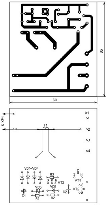
Encyclopedia of radio electronics and electrical engineering / Clocks, timers, relays, load switches The article proposes a version of the device that automatically supplies power to the slave device when the master is turned on. There are cases when electrical and radio devices work together, for example, a TV and an antenna amplifier. Therefore, it is desirable to turn them on and off in a certain sequence, first - the master device (TV), then - the slave (amplifier). The proposed device, after turning on the master device, supplies mains voltage to the slave. With minor modifications, it can supply any power to the driven load, including those that do not have a galvanic connection with the mains. The scheme of the device is shown in fig. 1. It consists of a current transformer T1, a bridge rectifier on diodes VD1-VD4 with a smoothing capacitor C1. To connect power to the driven load, powerful field-effect switching transistors VT1 and VT2 are used.
If the driving load is turned off or is in standby mode with low current consumption, there is no voltage on the capacitor C1 or it is low. Therefore, all transistors are closed and the driven load is de-energized. After turning on the leading load, the current it consumes flows through the primary winding of the transformer T1, and an alternating voltage appears in the secondary, which rectifies the bridge rectifier. If the current of the primary winding exceeds a certain value, the voltage across the capacitor C1 will be sufficient to open the zener diode VD6. And when the voltage across the resistor R1 exceeds 0,6 ... 0,7 V, the transistor VT3 will open. In this case, the voltage on the capacitor C1 - a little more than six volts - through the transistor VT3 will go to the gates of the transistors VT1, VT2, which will open, and the mains voltage will go to the driven load. If the voltage on capacitor C1 exceeds 11,2 V, both zener diodes will open and therefore the voltage at the rectifier output will be limited. All elements are mounted on a printed circuit board made of fiberglass foiled on one side with a thickness of 1,5 ... 2 mm, the drawing of which is shown in Fig. 2. The device uses resistors C2-23, MLT, oxide capacitor - imported, ceramic - K10-17, diodes - any low-power rectifier, zener diodes - low-power with a stabilization voltage of 5 ... 7 V. Field-effect transistors IRF840 can be replaced with IRF640, and if the driven load power does not exceed 500 W, then IRFBC40 transistors. If the driven load current is more than 1 A, the transistors should be provided with heat sinks. We will replace the KT361B transistor with any of this series. Connector X1 - screw terminal block with a lead pitch of 7,5 mm, designed for installation in the holes of the printed circuit board.
The current transformer is made from a step-down transformer of a small-sized power supply (120/12 V 200 mA). The active resistance of its primary winding is 200 ohms. The windings of this transformer are wound in separate sections, which simplifies rework. Its primary winding is included as a secondary winding, and the secondary is removed, and the primary winding wire is wound in its place. For the manufacture of a current transformer, any low-power serial step-down transformer is also suitable, for example, the TP-121, TP-112 series. By selecting the number of turns of the primary winding, the threshold value of the current of the leading load is set, at which the driven load is turned on. For a load with a power of 50 W, the primary winding must contain four turns. The wire of this winding must be in reliable insulation and rated for the current consumed by the leading load. The appearance of the mounted board is shown in fig. 3. It is desirable to place it in a plastic case of a suitable size. Sockets for connecting loads are installed on the walls of the case.
If the driven load is low-voltage and high-current, and also does not have a galvanic connection with the 220 V network, the device diagram must be changed, as shown in color. To do this, the printed conductor is cut on the board, connecting pins 1 and 3 of the X1 connector, the drain of the transistor VT1 is disconnected from the XP1 plug and connected with a wire to pin 3 of the X1 connector. Field-effect transistors IRF840 are replaced with powerful low-voltage ones, for example, IRFZ44 or similar. Author: I. Nechaev
Machine for thinning flowers in gardens
02.05.2024 Advanced Infrared Microscope
02.05.2024 Air trap for insects
01.05.2024
▪ Sony MDR-HW9.1DS 700 Wireless Headphones ▪ Acer Nitro V 16 gaming laptop ▪ Improving the Reliability of Powerful Silicon Carbide Semiconductors
▪ section of the site Personal transport: land, water, air. Article selection ▪ article Electric helicopter. Tips for a modeller ▪ article Which countries were originally called the third world? Detailed answer ▪ article Head of the Bureau of Planning and Accounting of the Sales Department. Job description
Home page | Library | Articles | Website map | Site Reviews
www.diagram.com.ua |


 Leave your comment on this article: