|
|


 Arabic
 Bengali
 Chinese
 English
 French
 German
 Hebrew
 Hindi
Hindi Italian
 Japanese
 Korean
 Malay
Malay Polish
 Portuguese
 Spanish
 Turkish
 Ukrainian
 Vietnamese
|
ENCYCLOPEDIA OF RADIO ELECTRONICS AND ELECTRICAL ENGINEERING Once again about the power supply of the digital multimeter from the network. Encyclopedia of radio electronics and electrical engineering
Encyclopedia of radio electronics and electrical engineering / Power Supplies The topic of mains power supply for compact digital multimeters is not new; it has been repeatedly raised on the pages of amateur radio literature. In particular, this issue was studied in detail in [1]. The power supply of the multimeter must provide galvanic isolation of the output circuit from the mains with a small (no more than 20 ... 30 pF) throughput capacitance, be simple and compact. The currently optimal structure of a mains power supply for a multimeter is a stabilized buck-to-dc converter with a transformer operating at an increased (tens and hundreds of kilohertz) frequency. Among the many similar designs, for example, the device [2] enjoys well-deserved popularity among radio amateurs. In the author's opinion, the weak point of such sources is a high-frequency transformer, which has to be manufactured independently. However, this is the most critical part of the converter. It is on its quality that 1 depends both the correct operation of the multimeter and the safety of working with it. Knowing this, some radio amateurs who do not have the skills to manufacture transformers simply do not undertake to repeat such devices so as not to risk expensive devices. One of the ways to achieve good repeatability of any design is the absence of self-manufactured or scarce parts in its composition. This approach is also favorable for a number of other design qualities - reliability, ease of manufacture, maintainability.
In view of the foregoing, the author has developed and offers radio amateurs his own version of a mains power supply for a portable digital multimeter. The device is simple and does not require adjustment. Main Specifications
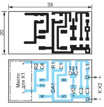
The device, the scheme of which is shown in fig. 1 is a two-stage AC/DC converter. The output voltage parameters necessary to power the multimeter in it are formed by a linear integrated stabilizer DA2. The first stage of the converter is a ready-made device that almost everyone has today - a cell phone charger with an output voltage of 5 V (A1). Through the X1 connector, its voltage is fed to the input of the second boost converter A2 - microassembly PSD-0512ELF (DA1), operating at a frequency of about 100 kHz. The voltage at the output of this microassembly is 12 V, and its output circuit is isolated from the input circuit. It is the parameters of this insulation that are indicated in the main technical characteristics of the device. In fact, they are even higher, since the output circuit of the charger is also isolated from the network. An additional advantage of the described structure is the ability to power the multimeter from any source of constant voltage of 5 V, including from the device being tested by the multimeter. Resistor R2 provides the initial load of the charger until the DA1 microassembly converter starts working. Resistor R1 serves as the minimum load for this microassembly, because the current consumed by the main load (multimeter) is small and depends on the multimeter's operating mode, and no-load operation is contraindicated for the microassembly. The output voltage of the microassembly is fed to the integral stabilizer (DA2), which lowers it to 9 V. From the output of the stabilizer, the voltage is applied to the multimeter through the C2L1C3 low-pass filter with a cutoff frequency of about 50 kHz, which prevents high-frequency interference from the DA1 microassembly from penetrating the multimeter and the device under test. Capacitor C2, in addition, eliminates the possible self-excitation of the stabilizer DA2. A few words about the choice of integrated stabilizer DA2. The ideal option would be to use the 78L09 microcircuit with an output voltage of 9 V here. However, these microcircuits are not in great demand today, so stores often simply do not order them, as a result of which they are found on sale. Therefore, a more common integrated stabilizer of the 78L05 series was used, the stabilization voltage of which was 5 V increased to 9 V by including a zener diode VD1 common wire in the circuit. Since this zener diode has a nominal stabilization voltage of 3,6 V, the voltage at the output of the DA2 stabilizer increases, strictly speaking, only up to 8,6 V, but this is quite enough for the multimeter to work. The parts of the source (with the exception of the cell phone charger) are placed on a 39x20 mm printed circuit board, the drawing of which is shown in fig. 2. Please note that the X1 connector is missing from the drawing, only a place is left for its installation.
The fact is that it is supposed to use a charger with a standard connector connected to a cell phone, and this connector may be different for different phones. Therefore, when starting to manufacture the described device, you must first determine the type of the desired connector, find the same one, and correct the printed circuit board drawing to accommodate it. This will make it possible to use the charger both for its intended purpose (for charging the phone battery) and for powering the multimeter. Connector X2 - block from the used battery "Krona". All resistors and capacitors are size 1206, inductor L1 is SQC322520T-100K-N size 1210. The finished printed circuit board is mounted in the battery compartment of the multimeter in any convenient way. PCB file in Sprint Layout 5.0 format can be downloaded from ftp://ftp.radio.ru/pub/2016/12/bp-mult.zip. Literature
Author: A. Savchenko
Machine for thinning flowers in gardens
02.05.2024 Advanced Infrared Microscope
02.05.2024 Air trap for insects
01.05.2024
▪ Moving objects with light rays ▪ Robots instead of astronauts
▪ site section Power supplies. Article selection ▪ article I'm going, I'm going, I don't whistle, but when I hit, I won't let go. Popular expression ▪ Fritter article. Job description ▪ article Casein paints on soluble glass. Simple recipes and tips ▪ article Plate - grinding wheel. Focus secret
Home page | Library | Articles | Website map | Site Reviews
www.diagram.com.ua |


 Leave your comment on this article: