|
|


 Arabic
 Bengali
 Chinese
 English
 French
 German
 Hebrew
 Hindi
Hindi Italian
 Japanese
 Korean
 Malay
Malay Polish
 Portuguese
 Spanish
 Turkish
 Ukrainian
 Vietnamese
|
ENCYCLOPEDIA OF RADIO ELECTRONICS AND ELECTRICAL ENGINEERING Laboratory power supply on integrated voltage stabilizers, 220 / 1,25-27 volts 3 amperes + 0-±24 volts 0,6 amperes. Encyclopedia of radio electronics and electrical engineering
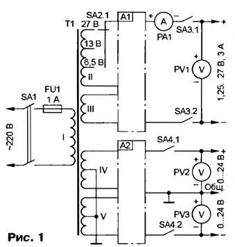
Encyclopedia of radio electronics and electrical engineering / Power Supplies The article brought to the attention of readers describes a laboratory power supply made on microcircuits - voltage stabilizers. It contains two independent sources: a powerful one with an output voltage of 1,25 to 27 V and a maximum load current of 3 A, and a relatively low-power bipolar one with a voltage of 0..±24 V and a current of up to 0,6 A. The laboratory power supply (Fig. 1) consists of two independent sources A1 and A2, galvanically not connected to each other, and has a wide range of capabilities.
Main Specifications
The device uses a network transformer T1 common to both sources. The output voltage and load current of a more powerful source A1 can be controlled using a voltmeter and ammeter, which are made on the basis of the M2001 pointer device. In the author's version, the output voltage of source A2 is measured by two identical digital voltmeters assembled on the basis of the ADC KR572PV2A. Diagrams of such devices have been repeatedly published on the pages of "Radio", for example, in the article [1], so we will not dwell on them in detail here. Block A1 is a stabilizer, which is described in [2], made on domestic elements and modified by the author. The work consists in the possibility of stepwise regulation of the output voltage intervals in order to reduce losses on the regulating transistor. This unit can be used to power various equipment and for repair work, as well as a charger. Power supply A1 provides a stabilized output voltage in the range of 1,25 ... 6,5; 1,25 ... 13 and 1,25 ... 27 V with the possibility of its smooth adjustment. The maximum load current (current protection level) can be set within 0,05 ... 3 A. If the set level is exceeded, the device automatically switches to the current stabilization mode, and after the overload is eliminated, it returns to the voltage stabilization mode. Block diagram A1 is shown in fig. 2.
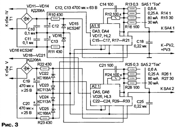
The device consists of the following functional parts: a powerful rectifier VD1-VD4 with a filter C1-C3; voltage regulator on the DA1 chip and the VT1 transistor; current protection unit at OS DA2; two auxiliary sources of stable voltage VD5VD6C4R1 and VT2VD7-VD9 to power the OS DA2. Switch SA2 sets the required interval for regulating the output voltage. If the load current does not exceed 50 mA, the device works as a stabilizer, connected according to the typical scheme [3]. When the load current exceeds this value, the voltage drop across the resistor R2 opens the transistor VT1, thereby limiting the current through the DA1 chip to 50 mA. Adjust the output voltage with a variable resistor R8. The current protection node works as follows. A stable output voltage is applied to the non-inverting input of the op-amp DA2. The sum of the output voltage and the voltage drop across the current-measuring resistor R3 is fed to its inverting input through an adjustable divider R6R4. Op-amp DA2 compares the output stabilized voltage with the voltage coming from the divider, which depends on the load current. As long as the voltage at the non-inverting input is greater than at the inverting input, the output of the op-amp is set to a high level close to the output voltage. Diode VD10 and LED HL1 are closed. The device operates in the voltage stabilizer mode. If the load current increases, the voltage drop across the current-measuring resistor R4 increases and at some point the voltages at the inputs of the op-amp become equal. After this, a further increase in the load current does not occur, since the output of the op-amp shunts the adjustment circuit of the DA1 stabilizer through the open diode VD10 and the HL1 LED. Resistor R5 limits the current through the HL1 LED and the op-amp at an acceptable level. In this case, the voltage drop across the resistor R4 is maintained constant by changing the output voltage across the load. The device enters the current stabilization mode, as evidenced by the on LED HL1. The level of load current limitation is set by a variable resistor R3. For normal operation of the device, it is necessary that the minimum voltage difference at the input (positive terminal of the capacitor C3) and the output of the stabilizer (pin 8 of the DA1 microcircuit) be not less than the sum of the minimum voltage drop on the DA1 microcircuit and the opening voltage of the emitter junction of the transistor VT1 (in our case, 3,8 .XNUMX V). The diagram of the bipolar voltage regulator A2 is shown in fig. 3.
The dash-dotted line marks the nodes A1.1 and A2.1, which coincide according to the scheme with A1.1 in Fig. 2. Node A2.1 differs from A1.1 in that instead of KR142EN12A, a negative polarity voltage regulator KR142EN18A [3] is used (it has pin 8 - input, 2 - output, 17 - control output), and the VD26 diode, HL3 LED and oxide capacitor C22 included in reverse polarity. The principle of operation of the device A2 is similar to block A1 (see Fig. 2). The difference lies in the fact that there is no powerful regulating transistor, there is no switch for output voltage limits, and the adjustment of the protection operation current is stepwise, using the SA5 switch and resistors R13-R16 and R25-R28. Protection operation current levels - 0,6 A, 0,25 A, 80 mA and 30 mA - are set in both channels simultaneously. The output voltage is adjusted from zero due to the supply of a bias voltage in the adjustment circuit of the stabilizers DA3 and DA5 separately in both channels. The voltage is regulated by variable resistors R20 and R32 from 0 to +24 V and from 0 to -24 V, respectively. The bias voltage is removed from the auxiliary source of stabilized voltage R22R23C19C20VD22-VD25. Transistor KT825A (VT1) can be replaced by any of this series. Transistor VT2 must be selected with an initial drain current of about 10 mA. The control transistor (KT825A) and integral stabilizers are installed on separate heat sinks or on the metal rear wall of the case. In the latter case, they should be securely insulated from the housing with mica gaskets. Measuring devices, LED indicators, controls, output terminals are placed on the front panel. The dimensions of the device depend mainly on the size of the network transformer, the power of which must be at least 180 watts. In the author's version, the mains transformer is self-made, made on a 120x60x32 mm tape toroidal magnetic circuit from a voltage stabilizer for tube TVs. The primary (network) winding contains 990 turns of PEL wire 0,4- Winding II (power for block A1) contains 145 turns with taps from the 50th and 82nd turns of PEL wire with a diameter of 1 mm. The voltage at the terminals of this winding is 11, 18 and 32 V at a current of at least 3,2 A. Winding III (auxiliary for block A1) consists of 45 turns of PEL wire 0,25. The voltage on the winding is 10 V at a current of 20 mA. Winding IV (power winding for block A2) contains 256 turns of PEL 0,56 wire with a tap from the middle. The voltage on it is 2x28 V at a current of at least 1 A. The V winding (auxiliary for block A2) consists of 110 turns of PEL 0,4 wire with a tap from the middle. The voltage on the winding is 2x12 V at a current of 50 mA. A properly assembled device does not need to be adjusted. It may be necessary to select separate copies of the OS. If desired, you can increase the output current of the sources by connecting in parallel the required number of regulatory elements - transistors in parallel VT1 in block A1 (current-leveling resistors with a resistance of 0,1 Ohm should be included in the transistor emitter circuit) and stabilizers in parallel to the DA3, DA5 microcircuits in block A2 (how to connect stabilizers in parallel , can be found in [4]). In this case, it is necessary to change the resistance of the current-measuring resistors accordingly and, of course, use a more powerful network transformer. The laboratory power supply, in addition to its direct purpose, can also perform additional functions. Block A1 can be used as a charger. The charging current is set by resistor R3 with the output terminals closed. The voltage on the battery (or battery) and the charging current are controlled using a voltmeter PV1 and an ammeter PA1, respectively. Using block A2, you can check the p-n junctions of low-power semiconductor devices, capacitors with a capacity of 0,1 microfarads and measure voltage. To check the p-n junctions, switch SA5 select the minimum allowable current. Resistor R20 (R32) set zero voltage at the output. To the output terminals "+" ("-") and "Common." connect, for example, a diode and gradually increase the voltage. If the diode is connected in the forward direction, the overcurrent indicator HL2 (HL3) will light up. In this case, the voltmeter will show the value of the forward voltage drop across the diode. If the diode is turned on in the opposite direction, the power supply mode will not change. In the case of checking the zener diode when turning it back on, the voltmeter will show its stabilization voltage. When checking capacitors, the SA5 switch also selects the minimum load current. Resistor R20 (R32) set the maximum, but not more than the nominal for a particular capacitor, the output voltage. A capacitor is connected to the output terminals (observing the polarity for oxide capacitors) and the SA4 switch is turned on. By the duration of the flash of the overload indicator, you can indirectly estimate the capacitance of the capacitor or detect its leakage. To measure the voltage during various experiments and repair work, you can use the unit's voltmeters. Before work, disconnect the device from the power supply by opening the contacts of the SA4 switch. It is convenient to supply voltage to the device under study from block A1. Literature
Author: A. Muravyov, village of Lesnoy, Ryazan region.
Machine for thinning flowers in gardens
02.05.2024 Advanced Infrared Microscope
02.05.2024 Air trap for insects
01.05.2024
▪ A young star is eating the planet ▪ Ecological way to recycle old solar panels ▪ NCP693 - new low power LDO regulator ▪ Bacteria will protect the foundation from subsidence
▪ site section And then an inventor (TRIZ) appeared. Article selection ▪ article Methods for assessing the severity of labor. Basics of safe life ▪ article Who, when and how first determined the size of the globe? Detailed answer ▪ article Even Ichthyander will approve. Personal transport
Home page | Library | Articles | Website map | Site Reviews
www.diagram.com.ua |


 Leave your comment on this article: