|
|


 Arabic
 Bengali
 Chinese
 English
 French
 German
 Hebrew
 Hindi
Hindi Italian
 Japanese
 Korean
 Malay
Malay Polish
 Portuguese
 Spanish
 Turkish
 Ukrainian
 Vietnamese
|
ENCYCLOPEDIA OF RADIO ELECTRONICS AND ELECTRICAL ENGINEERING Converter for powering household equipment
Encyclopedia of radio electronics and electrical engineering / Voltage converters, rectifiers, inverters For the attention of readers, we offer a description of a backup converter for powering household equipment in the absence of voltage in the lighting network. Its distinguishing feature is the presence of two conversion stages: high-frequency and low-frequency, which made it possible to significantly reduce the dimensions and weight of the device. Today there is an increased interest in the development and manufacture of powerful converters for powering various household equipment from batteries. This is largely due to two factors. Firstly, various kinds of restrictions and interruptions in power supply, which have recently become a common practice in many regions of the country. Secondly, modern achievements in the field of industrial production of specialized electronic components for converter technology. These include, first of all, powerful high-speed field-effect transistors with their inherent ease of control and low on-state losses, as well as a wide range of integrated PWM controllers, which are, in fact, single-chip converter control units. It is also important that recently such an element base has become available to an ordinary radio amateur, both in terms of nomenclature and cost. As a result, it became possible to develop converting devices containing a small number of parts and at the same time having high energy and operational characteristics. Descriptions of such converters have been published more than once on the pages of "Radio" [1, 2] and in the relevant technical literature [3, 4]. A distinctive feature of these devices is that they all operate at a low conversion frequency (usually 50 Hz). This is due to the need to ensure that the output parameters of the converters correspond to the frequency characteristics of the household electrical network, since there is a large class of electrical appliances that require an alternating supply voltage. These, for example, include all consumers containing a network transformer or various types of AC motors. At the same time, the choice of a low conversion frequency causes certain design and operational difficulties: the manufacture of a powerful output transformer, which mainly determines the weight and size parameters of the entire device, and the characteristic "hum" of the converter during its operation. In addition, the described converters, as a rule, are not equipped with output voltage stabilization units, depending on the power of the load connected to them or the degree of discharge of the supply battery. As a result, changes in the amplitude of the output alternating voltage are possible within a fairly wide range (up to 30 ... 40%), which does not always favorably affect consumers. All of the above predetermined the design of the proposed converter, which was developed taking into account the indicated disadvantages inherent in existing devices. Functionally, the converter consists of two main parts: a powerful high-frequency step-up inverter with an output rectifier and a low-frequency inverter-switch. Main Specifications
The scheme of the device is shown in fig. 1. The high-frequency inverter is made according to the scheme of a push-pull forward converter on transistors VT1 -VT4 and transformer T1. The advantages of this solution include a low level of ripple, a better use of switching transistors in terms of current and a higher efficiency than those of converters assembled in a bridge circuit. Damping elements VD2, VD3, R1, C3 are used to reduce the amplitude of voltage surges during switching and facilitate the operation of transistors.
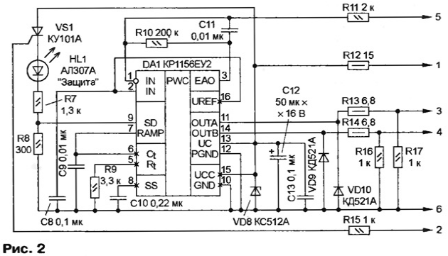
The protection of the inverter against overload or short circuit at the output is based on the current relay K1 included in the primary power circuit. It is made on the basis of a reed switch with one group of closing contacts, placed in the center of the coil, twisted from one or two turns of the supply wire coming from the positive terminal of the battery. At the same time, the internal resistance of such a relay is very small and has practically no effect on the operation of the converter in the normal mode. In the event of an overload, the contacts of the reed switch are closed, giving the corresponding signal for the protection operation to the control unit of the HF inverter A1. The speed of the current protection is 1...2 ms. The output voltage rectifier is made according to the bridge circuit on diodes VD4-VD7, which also allows to reduce the level of ripples and increase the utilization factor of the pulse transformer T1. The rectified voltage is supplied to the smoothing filter L1C5-C7. The voltage feedback signal required for the operation of the RF inverter control unit A1 is removed from the resistive voltage divider R3-R5. A stabilized DC voltage is supplied to a low-frequency inverter-switch, made according to the full bridge circuit on transistors VT5-VT8. The alternating voltage of the rectangular shape of the mains frequency generated by the switch is supplied to the load of the converter. The operating mode of the switch determines the control unit of the LF inverter A2. The transistors VT5-VT8 are controlled by identical drivers A4-A7, galvanically isolated from the rest of the converter. The "heart" of the RF inverter is the KR1156EU2 [5] PWM controller microcircuit (foreign analogue - UC3825 from Unitrode [6]), which is designed specifically to control push-pull switching power supplies with a high switching frequency, operating with voltage or current feedback. The scheme of the control unit of the HF inverter A1 is shown in fig. 2.
The frequency of the controller's internal master oscillator is determined by the ratings of the external elements - resistor R9 and capacitor C9, and at the indicated values it is approximately 50 kHz. The sawtooth signal necessary for operation, formed on the capacitor C9, is fed to the RAMP input of the microcircuit. A voltage from a reference source of +5 V is applied to the direct input IN of the error signal amplifier (USO) inside the microcircuit. The USO gain in the low-frequency region depends on the resistance of the resistors R4, R7 and is equal to 3. Capacitor C5 is designed to correct the frequency response of the amplifier in the high-frequency region in order to increase the stability of the entire pulse-width control system. The change in the width of the output control pulses occurs as a result of comparing the internal comparator of the sawtooth voltage controller acting at the RAMP input with the output voltage of the USO. The generated control pulses with a repetition rate of 25 kHz from the outputs OUTA and OUTB are fed to transistors VT1, VT2 and VT3, VT4, respectively. Capacitor C10 determines the operation of the controller soft start node. At the moment the power is turned on, the capacitor starts charging from the source with a current of 9 μA, while the voltage increase at the SS pin as it charges ensures a smooth increase in the duration of the controller's operating cycle. As can be seen from the main circuit (see Fig. 1), in the event of an overload of the converter, the current relay K1 is activated, closing the contacts of the reed switch K1.1. This opens the trinistor VS1, causing the HL1 "Protection" LED to turn on, as well as the appearance of a voltage drop of about 2 V across the resistor R8. This voltage is applied to the input of the SD controller, thereby putting it into blocking mode. The outputs OUTA, OUTB of the DA1 chip are switched to a high-impedance state, and the switching transistors VT1-VT4 are closed. In order to return the device to the operating state after the overload has been eliminated, it will be necessary to turn off the power to the converter for a while. The parametric stabilizer R12VD8 limits the controller supply voltage to 12 V. The driver power supply unit A2 is a low-power pulse converter, made according to the scheme of fig. 3.
On the logical elements DD1.1, DD1.2, a master oscillator is assembled that generates pulses with a repetition rate of about 100 kHz. This is followed by a frequency divider by 4, made on the triggers of the DD2 chip. Pulses from the inverse outputs of the triggers DD2.1, DD2.2 and the direct output of the trigger DD2.2 are fed to the logic elements DD1.3 and DD1.4. From the outputs of these elements, the generated control pulses with a repetition rate of approximately 25 kHz are fed to the transistors VT9 and VT10, switching the current of the primary winding of the transformer T2. The diagram of the control unit for the low-frequency inverter A3 is shown in fig. four.
On the integral timer DA2, included according to the standard scheme, a master oscillator is assembled. The repetition frequency of the generated pulses is determined by the elements C17, R23, R24. For the specified ratings, it is 100 Hz. The signal from the generator is fed to a frequency divider by 2, collected on a DD3.1 trigger, which acts as a biphasic signal shaper. Further, from the shaper, pulses with a frequency of 50 Hz are fed to the logic elements DD4.1, DD4.2, from the output of which, through transistors VT11, VT12, they are fed to the corresponding LEDs of the driver optocouplers (A4-A7). A single vibrator assembled on a DD3.2 trigger is designed to obtain a pause between control pulses. The presence of such a pause is necessary to prevent the occurrence of a through current in the arms of the transistor bridge VT5-VT8. The duration of the formed pause is determined by the values of the elements C19, R25, R26, and for those indicated in the diagram it is about 1 ms. Drivers A4-A7 for controlling switching transistors VT5-VT8 of a low-frequency inverter are made according to identical circuits in Fig. 5.
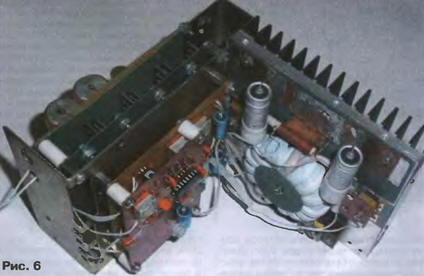
The control signal is fed to the driver through a diode optocoupler U1, which provides galvanic isolation from the LF inverter control unit. Further, after the amplifier on the transistor VT13, the signal enters the complementary output stage VT14VT15, loaded directly on the gate circuit of the switching transistor VT5. The driver is powered by a low-power pulse converter A2 through an isolation transformer T3 and a diode bridge VD15 with a smoothing filter C21. The R34VD14 circuit limits the maximum gate voltage of the field effect transistor to 15 V. In the author's version, the converter is assembled in a metal case of a suitable size - 200x120x120 mm. The appearance of the device is shown in fig. 6.
All functional units of the converter are assembled on separate printed circuit boards, with the exception of power elements. Particular attention should be paid to the topology of the PCB layout of the PWM controller, trying not to allow the close relative position of the conductors of the input and output circuits, and also, if possible, to minimize their length. I recommend that the printed circuit board for this assembly be made of double-sided foil fiberglass, using the foil on one side as a common wire. The heat-generating elements VT1 - VT4 of the high-frequency inverter, as well as the transformer T1, capacitors C1, C2 and damping elements VD2, VD3, R1, C3 are mounted on the rear wall of the case, made of a solid duralumin plate with dimensions of 120x120 mm and a thickness of 8 mm. Installation is made with a copper wire (tire) with a cross section of 10 mm2. The rear wall on the outer side is provided with vertically arranged ribs, thus, the effective area of the working surface of the resulting heat sink is about 600 cm2. The remaining space on the rear wall of the device is reserved for the terminals for connecting the battery and the fuse FU1. Transistors VT5-VT8 are equipped with small heat sinks, with an area of about 50 mm == 2 each. Instead of the IRFZ34N (VT1-VT4) transistors indicated in the diagram, IRFZ44, BUZ11, KP723A or any other MOSFET with an induced n-channel, a maximum drain current of at least 35 A, a maximum drain-source voltage of at least 55 V and an open channel resistance of no more than 0,04 ohm. Instead of transistors IRF820 (VT5-VT8), it is permissible to use IRF830, BUZ90, KP707B1 or other appropriate structures with a maximum drain current of at least 2 A and a maximum drain-source voltage of at least 400 V. Transistors KT972A (VT9-VT12) are replaceable by KT829A or composite KT315 + KT815 with any letter indices. In place of the rest of the transistors, you can use any low-power bipolar of the corresponding structure. Diodes KD226G (VD4-VD7) can be replaced by KD226D. Oxide capacitors C1, C2, C5, C6 - K50-24, K50-27, capable of operating in circuits with significant current ripples. The rest of the oxide capacitors used in the device are K50-6, K50-16, K53-14A, non-polar - any ceramic, for example, KM-5, KM-6, K10-17. Switch Q1 - any, designed for a rated current of at least 20 A. The current relay K1 is made on the basis of the KEM-1 reed switch or similar with one pair of make contacts, which has the shortest possible response time. The reed switch is placed in a thin-walled cylindrical tube of a non-magnetic material of suitable diameter. A relay winding containing one or two turns is wound over the tube. The exact number of turns is selected during adjustment. The inductor L1 is made on the basis of the B28 magnetic circuit made of M2000NM ferrite. A winding is wound on the coil frame until it is filled with PEV-2 0,9 wire. When assembling, a gasket made of non-magnetic material 0,1 mm thick is placed between the parts of the magnetic circuit. The inductance of such a choke is about 1 mH. Transformer T1 is wound on two ring magnetic cores K65x40x6 of M4000NM ferrite folded together. Winding I contains 2x6 turns of 60 PEV-2 0,35 conductors, and winding II - 220 turns of PEV-2 0,9 wire. Before winding, the sharp edges of the magnetic core should be rounded off. Winding II is wound first, turn to turn. Then interwinding insulation is laid, on top of which winding I is placed. To reduce the leakage inductance, it is wound in two wires (two bundles of 60 conductors each) and evenly distributed over the magnetic circuit. For the primary winding, you can use a bundle formed from a copper shielding braid of a coaxial cable of a suitable (5 ... 7 mm2) section. To provide inter-turn insulation, the bundle is placed in a tube of insulating material (for example, PVC) of a suitable diameter. The midpoint of the primary winding is obtained by connecting the beginning of one half-winding to the end of the other. The T2 transformer is made on a K28x16x9 ring made of M2000NM ferrite. The windings contain: primary - 2x20, and secondary - 20 turns of wire PEV-2 0,4. First, they wind, as in the T1 transformer, the secondary winding, and on top of it - in two wires - the primary. By connecting the beginning of one half-winding to the end of the other, a midpoint is obtained. Each TK driver power transformer (four will have to be made) is wound on a K20x12x6 ring made of M2000NM ferrite. The windings contain: primary - 30, secondary - 40 turns of wire PEV-2 0,28. The secondary winding is wound first. To establish the converter, you will need a 10 ... 15 V DC source with an output current of 5 ... 10 A. For this purpose, you can use a car battery charger, preferably equipped with output current overload protection. The high-frequency and low-frequency parts of the converter are adjusted separately. After assembling the high-frequency part of the device, you should make sure that the installation is correct and of high quality. Then the engine of the variable resistor R4 is set to the upper position according to the diagram. Power is supplied to the device through a current-limiting resistor with a resistance of 10 ohms and a power of 5 W. In this case, the no-load current should not exceed 300 mA, and the voltage at the output of the VD4-VD7 rectifier should be in the range of 190 ... worked at a current of about 200 A. After that, the current relay is connected to the device and the high-frequency part is adjusted, feeding it from the battery. Gradually increasing the power of the load connected to the VD4-VD0,5 rectifier up to 25 W, they control the consumed current, output voltage and thermal mode of the converter. During long-term operation, the temperature of the heat sink should not exceed 4 °C. On this, the establishment of the high-frequency part of the device can be considered complete. The power supply unit of the drivers and the drivers themselves do not need to be adjusted during error-free installation. Establishing the control unit for the low-frequency inverter consists in setting the frequency of the clock generator (100 Hz) with a tuning resistor R23 and the duration of the pause between the output pulses (about 1 ms) with a tuning resistor R26. After assembling the entire low-frequency part of the converter, a constant voltage of 10 ... 15 V is applied to its input (taking into account the polarity), while controlling the output alternating voltage across the resistor R6 using an oscilloscope. The observed output signal should be square-wave, symmetrical with a duty cycle of 2, with no visible distortion. If necessary, make an additional adjustment of the duration of the pause between the half-periods of the meander with a tuning resistor R26. This completes the adjustment of the low-frequency part of the converter. Further, the high-frequency and low-frequency parts are connected to each other and the performance of the converter is monitored as a whole in the entire power range, if necessary, adjusting the output alternating voltage of 220 V with a variable resistor R4. The output voltage should be measured with a pointer device showing the effective (effective) value! In conclusion, I would like to note that the proposed device can be easily adapted to the required output characteristics. By selecting the division factor of the resistive divider R3-R5, it is possible to set a different output voltage (for example, 127 V), and by changing the values of the elements C17, R24, you can get other values \u400b\uXNUMXbof the output frequency (for example, XNUMX Hz). Literature
Author: I.Poley, Yuzhno-Sakhalinsk
Machine for thinning flowers in gardens
02.05.2024 Advanced Infrared Microscope
02.05.2024 Air trap for insects
01.05.2024
▪ Premium electric car Mercedes-Benz EQS ▪ Robomobiles for highway construction ▪ Smartphone flat camera technology
▪ site section Clocks, timers, relays, load switches. Article selection ▪ article Great helmsman. Popular expression ▪ article Do insects have blood? Detailed answer ▪ article Animal care worker in a terrarium. Standard instruction on labor protection ▪ article Spectacular tricks and their clues. Encyclopedia
Comments on the article: Peter Do you have boards for this inverter?
Home page | Library | Articles | Website map | Site Reviews
www.diagram.com.ua |


 Leave your comment on this article: