|
|


 Arabic
 Bengali
 Chinese
 English
 French
 German
 Hebrew
 Hindi
Hindi Italian
 Japanese
 Korean
 Malay
Malay Polish
 Portuguese
 Spanish
 Turkish
 Ukrainian
 Vietnamese
|
ENCYCLOPEDIA OF RADIO ELECTRONICS AND ELECTRICAL ENGINEERING Stabilized VIPER-switched SMPS - from charger
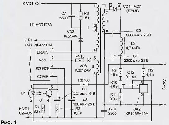
Encyclopedia of radio electronics and electrical engineering / Power Supplies In the author's article "ViPer-100A and "pocket" charger based on it"(" Radio ", 2002, No. 11) a device for charging car batteries was described. How to turn it into a stabilized power source by a simple modification is described in the proposed article. In [1], a VIPer-100A chip charger was described that provides the necessary charging current for the battery at the beginning and the voltage on it at the end of charging. During the development of special requirements for its parameters were not presented. However, it is possible, with a simple modification, to turn this charger into a stabilized power source with very high performance. To do this, we turn to the SMPS computer-aided design program based on VIPer microcircuits [2] and at the stage of determining the output filter Output Type (see Fig. 9 in [2]), instead of the established Direct, we will choose Self - a standard U-shaped LC filter. Therefore, we will have to tighten the requirements for the voltage ripple value at the output of the device - in the Output Ripple section in the First Cell Ripple window, set 0,5 V and Second Cell Ripple - 0,02 V. On the program toolbar DS (see Fig. 6 in [2]), let's change the Primary Regulation to Secondary Regulation. As a result, the SMPS circuit shown in Fig. 2 in [1] will change somewhat. A fragment of the modified scheme is shown in Fig. 1. The numbering of the elements continues the previously accepted one. Resistors R5R6 and microammeter PA1 are excluded.
The essence of the changes comes down to the introduction of a secondary control loop into the SMPS, due to which the source parameters are significantly improved: at an output voltage of 13,6 V and a rated load current of 6 A, the output voltage ripple amplitude will not exceed 15 mV. This is achieved by adding a DA2 chip and an optocoupler U1 to the device. Especially noticeable is the improvement in the stabilizing properties of the SMPS according to its load characteristic, shown in Fig. 2 (compare with Fig. 4 in [1]).
The speed in the secondary control loop (it depends on the gain of the Gain Optocoupler) is determined by the resistor R8. There is also a fundamentally new property of the modified SMPS - the ability to control the soft start time Soft Start Time, which depends primarily on the capacitance of the capacitor C6. By default, DS sets the optocoupler gain and soft start time to 1 and 10 ms, respectively. Let's leave the "soft" start time for the upgraded SMPS unchanged, and increase the optocoupler gain to 2, for which we turn to the VIPer and Regulation Parameters window (see Fig. 8 in [2]) and reset the required parameter. The ratings of the elements of the secondary control loop, calculated by the program, and then refined during the adjustment of the device, are shown in fig. 1. In the process of regulation, depending on the output voltage of the SMPS, the gain of the error signal amplifier in the PWM controller changes. To do this, the emitting diode of the optocoupler U1 is connected to the output of the device through a series-connected current-limiting resistor R8 and the DA2 microcircuit. Resistor R12 - ballast in the power supply circuit of the stabilizer DA2, and capacitor C12 - noise suppression in the control circuit. Resistive divider R9 - R11 set the operating point by choosing the initial current of the optocoupler diode. The luminous flux emitted by the diode regulates the current, and, accordingly, the equivalent resistance of the collector-emitter section of the phototransistor connected in parallel to the compensation circuit R2C6. We assume that under the influence of destabilizing factors, the output voltage of the SMPS will increase. Accordingly, the voltage at the control input (pin 1) of the DA2 chip and the current flowing through it will increase. Therefore, the current of the emitting diode will also increase, and the equivalent resistance of the collector-emitter section of the phototransistor will decrease. Reference materials [3] in fig. Figure 10 shows a graph illustrating the dependence of the voltage gain of the error signal amplifier A3 (see Fig. 1 in [1]), which, with a decrease in resistance in the compensation circuit, can decrease by 27 dB or more compared to the originally set one. Thus, when the resulting resistance in the compensation circuit changes, the error signal amplifier, by correcting the parameters of the switching pulses, restores the previous voltage value at the output of the SMPS. An additional feedback node of the SMPS is assembled on a small (17,5x25 mm) piece of the board for prototyping. Connect it to the charger through the L2 choke, and replace the capacitor C9 on the charger board with another, larger (6800 uF) capacitance. The inductor contains 22 turns of wire PEV-2 1,5, wound turn to turn on a mandrel with a diameter of 3,8 mm, its magnetic conductor - two ferrite tubes with a diameter of 3,5 and a length of 20 mm, used in high-frequency chokes. The top output of the inductor according to the scheme is soldered into the hole on the memory board, intended for the resistor R6. In addition, the conductor connects the negative outputs of the memory and the additional node. The collector and emitter circuits of the phototransistor are connected respectively to the compensation input (pin 5) and pin 4 of the PWM controller with a twisted pair of MGTF conductors. Trimmer resistor R10 - SPZ-19A or other small-sized, capacitors C6-K53-30 or K53-19, C12 - KM-5, resistors - OMLT. The domestic chip KR142EN19A is replaceable by a foreign analogue TL431. A stabilized power supply requires almost no adjustment. Before the first switching on of the SMPS after completion, the engine of the tuning resistor R10 is set to the lower position according to the diagram, a load equivalent is connected to the output of the source, and then it is connected to the network. By smoothly moving the engine up the circuit, they measure the voltage at the load, and as soon as it abruptly decreases from 15,3 to 13,6 V, the adjustment is stopped. In the future, the voltage at the load will be stably maintained at this level. The current of the emitting diode of the optocoupler at this moment should be equal to 1 ... 2 mA, which is much less than the maximum allowable (15 mA). This allows us to hope for high reliability of the developed device. Note that to improve noise immunity, DS "recommends" between pins 4 and 5 of the DA1 chip to connect a capacitor with a capacity of 1000 ... 2000 pF. On the STMicroelectronics website at a FAQ section (Frequently Asked Questions - frequently asked questions) has been placed, in which those who wish can find answers to questions related to the calculation of SMPS based on VIPer series microcircuits. The same section, translated into Russian by the author, with some additions. Literature
Author: S. Kosenko, Voronezh
Machine for thinning flowers in gardens
02.05.2024 Advanced Infrared Microscope
02.05.2024 Air trap for insects
01.05.2024
▪ Mobile workstation Tornado F7 Server Edition ▪ Small insects do not try to mimic perfectly ▪ The level of mercury will show the mobile phone ▪ A simple way to extract uranium from seawater ▪ TDA8939TH - class D digital amplifier
▪ section of the site The most important scientific discoveries. Article selection ▪ article Manufacture of caterpillars. Tips for a modeller ▪ What was the impetus for the Latin American Wars of Independence? Detailed answer ▪ article The functional composition of Thomson TVs. Directory ▪ article Conceived number. Focus secret
Home page | Library | Articles | Website map | Site Reviews
www.diagram.com.ua |


 Leave your comment on this article: